Simulation method, simulation program, and semiconductor manufacturing apparatus
What is AI technical title?
AI technical title is built by Patsnap AI team. It summarizes the technical point description of the patent document.
A simulation method, semiconductor technology, applied in semiconductor/solid-state device manufacturing, CAD numerical modeling, complex mathematical operations, etc., can solve problems such as sensor deterioration and high emission intensity
Inactive Publication Date: 2013-06-05
SONY CORP
View PDF3 Cites 0 Cited by
Summary
Abstract
Description
Claims
Application Information
AI Technical Summary
This helps you quickly interpret patents by identifying the three key elements:
Problems solved by technology
Method used
Benefits of technology
Problems solved by technology
[0011] Although ultraviolet light having a wavelength of 254nm is used for cleaning, there is a problem that if monitoring is directly performed, the sensor immediately deteriorates due to high emission intensity
Method used
Image
Click on the blue label to locate the original text in one second.
Reading with bidirectional positioning of images and text.
Examples
no. 1 example
[0081] 2. First embodiment (simulation method)
[0082] 3. The second embodiment (simulator)
[0083] 4. The third embodiment (dry etching device)
[0087] First, an outline of the present disclosure will be described before describing specific embodiments.
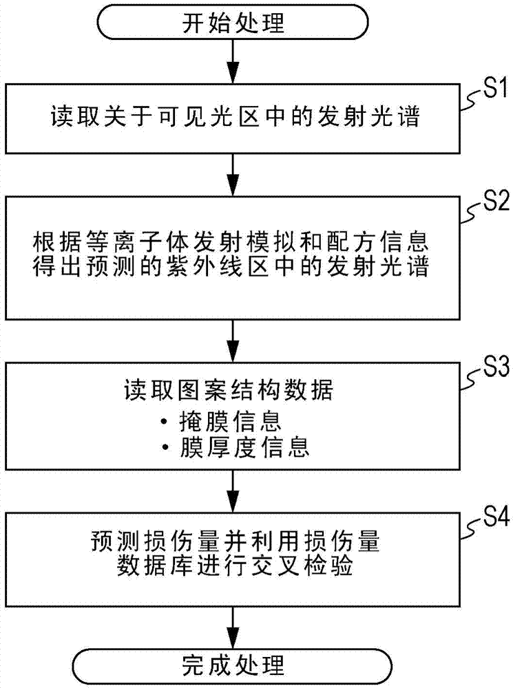
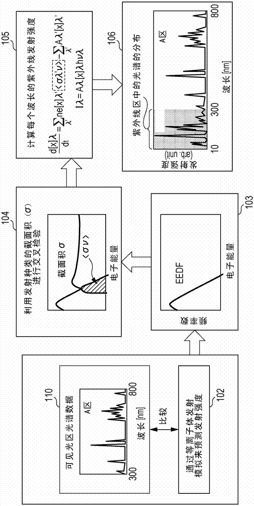
[0088] According to an embodiment of the present disclosure, the ultraviolet emission spectrum is predicted by performing simulations based on data of the visible emission spectrum without directly monitoring the ultraviolet emission.
[0089] Furthermore, the amount of damage to the film is predicted by performing simulation using the result of prediction of the ultraviolet emission spectrum by the simulation as input information.
[0090] Furthermore, for the purpose of reducing damage due to ultraviolet rays in real time, a semiconductor manu...
[0374] First, an outline of the present disclosure will be described before describing specific embodiments.
[0375] According to an embodiment of the present disclosure, the ultraviolet emission spectrum is predicted by performing simulations based on data of the visible emission spectrum without directly monitoring the ultraviolet emission.
[0376] Furthermore, the amount of damage to the film was predicted using the result of prediction of the ultraviolet emission spectrum by simulation as input information.
[0377] Furthermore, in order to reduce damage due to ultraviolet rays in real time, a semiconductor manufacturing device on which software based...
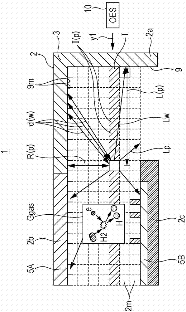
technical field [0001] The present disclosure relates to a simulation method and a simulation program for predicting the amount of damage due to ultraviolet rays in the manufacture of semiconductor devices. Furthermore, the present disclosure relates to a semiconductor manufacturing apparatus that predicts the amount of damage due to ultraviolet rays and controls process conditions. Background technique [0002] In the manufacture of semiconductor devices, a process using plasma generated by applying a high-frequency bias voltage has been widely used. [0003] In the plasma, particle collisions and interactions with chamber walls occur and, depending on the structure and process conditions of the processing chamber, ions, radicals and light are generated. [0004] Regarding technological development for predicting and controlling damage to a film (crystal defect) caused when the film is irradiated with ions, various techniques have been proposed, such as simulation methods,...
Claims
Application Information
Patent Timeline
Application Date:The date an application was filed.
Publication Date:The date a patent or application was officially published.
First Publication Date:The earliest publication date of a patent with the same application number.
Issue Date:Publication date of the patent grant document.
PCT Entry Date:The Entry date of PCT National Phase.
Estimated Expiry Date:The statutory expiry date of a patent right according to the Patent Law, and it is the longest term of protection that the patent right can achieve without the termination of the patent right due to other reasons(Term extension factor has been taken into account ).
Invalid Date:Actual expiry date is based on effective date or publication date of legal transaction data of invalid patent.

