Wafer-level packaging structure for improving response rate of thermopile infrared detector

An infrared detector, wafer-level packaging technology, applied in electrical radiation detectors, measuring devices, microstructure technology, etc. The effect of multiple losses, improved utilization, and improved response rate

Active Publication Date: 2013-06-12
北京中科微知识产权服务有限公司
View PDF4 Cites 16 Cited by
  • Summary
  • Abstract
  • Description
  • Claims
  • Application Information

AI Technical Summary

Problems solved by technology

[0005] However, since the silicon base material has a certain selectivity to the infrared band, and the transmittance of the original silicon base is not high, there is an infrared reflection phenomenon on the silicon surface, which will cause the infrared radiation energy to attenuate
In addition, the material of the suspension film 3 has a low absorption rate of infrared rays, causing secondary attenuation of infrared radiation energy, which limits the wavelength of the detector and lowers the responsivity.

Method used


Image

  • Wafer-level packaging structure for improving response rate of thermopile infrared detector
  • Wafer-level packaging structure for improving response rate of thermopile infrared detector
  • Wafer-level packaging structure for improving response rate of thermopile infrared detector

Examples


Embodiment 1

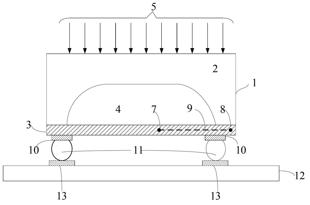
[0025] Embodiment one, such as figure 2 As shown, a thermopile infrared detector 1 includes a silicon substrate 2 , a suspension film 3 , and a cavity structure 4 , wherein the suspension film 3 contains a thermopile structure 9 .

[0026] The thermopile structure 9 is made inside the suspension membrane 3 through the existing technology, and the thermopile structure 9 is usually formed by a series of thermocouple bars connected in series. One end of the thermopile structure 9 is a hot end 7 and the other end is a cold end 8 .

[0027] An infrared anti-reflection film 6 is grown on the back of the silicon substrate 2 facing the infrared radiation source 5. In this embodiment, the infrared anti-reflection film 6 is uniformly grown on the back of the silicon substrate 2 directly by coating technology. Commonly used coating methods include vacuum evaporation, chemical phase deposition, sol-gel coating and other methods.

[0028] Then, lead electrodes 10 are drawn out on the sus...

Embodiment 2

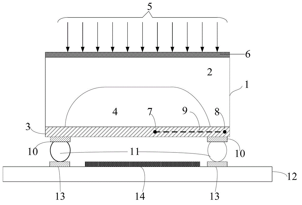
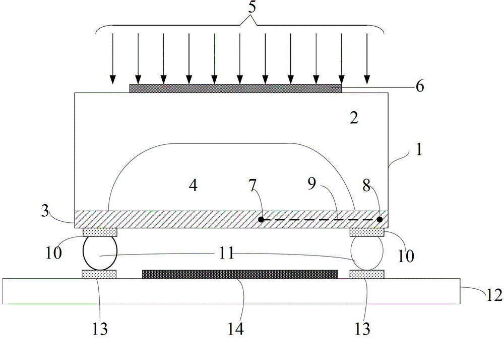
[0031] Embodiment two, such as image 3 As shown, it is a further improvement on the basis of Embodiment 1. The infrared anti-reflection coating 6 in the corresponding area on the back of the silicon substrate 2 above the cold end 8 is removed, so that the patterned infrared light is formed on the back of the silicon substrate 2. AR coating. The patterned infrared anti-reflection film covers the back area of ​​the silicon substrate 2 above the cavity structure 4 . The structure in other aspects is the same as in Embodiment 1. The detailed process of forming a patterned infrared anti-reflection coating is as follows:

[0032] The infrared anti-reflection film 6 is evenly grown on the back side of the silicon substrate 2 facing the infrared radiation source 5 by coating technology, and the photoresist is spin-coated on the surface of the infrared anti-reflection film of this layer, and then the anti-reflection film position needs to be removed (the cold of the thermopile The ...


PUM


Abstract

The invention provides a wafer-level packaging structure for improving a response rate of a thermopile infrared detector. The wafer-level packaging structure comprises an infrared detector and a bearing base plate for bearing the infrared detector; the infrared detector comprises a silicon substrate, a floating film, a cavity structure and a thermopile structure, wherein the cavity structure is formed in the silicon substrate; the thermopile structure is formed in the floating film; one end of the thermopile structure is a hot end; the other end of the thermopile is a cold end; a lead-wire electrode is led out on the floating film; a welding flux convex point is formed on the lead-wire electrode; and the infrared detector is buckled and stacked on the bearing base plate in an inverted manner. The wafer-level packaging structure is improved as follows: an infrared antireflection film is grown on the back surface of the silicon substrate of the infrared detector, and an infrared reflective film is arranged on the surface of the bearing plate directly opposite to the floating film below the cavity structure. The wafer-level packaging structure is further improved as follows: the infrared antireflection film is a graphical infrared antireflection film which is covered on the back surface of the silicon substrate except a corresponding area of the back surface of the silicon substrate above the cold end. The wafer-level packaging structure is used for improving the response rate of the infrared detector.

Description

technical field [0001] The invention relates to a microelectronic packaging structure, in particular to a wafer-level packaging structure of a thermopile infrared detector. Background technique [0002] Infrared detectors are one of the most critical components in an infrared system. The thermopile infrared detector is an uncooled infrared detector developed earlier. Its working principle is based on the Seebeck effect, in which a temperature difference between two different electrical conductors or semiconductor materials results in a voltage difference between the two materials. Because thermopile infrared detectors have the advantages of small size, can work at room temperature, wide-spectrum infrared radiation response, can detect constant radiation, and low manufacturing cost, they are widely used in safety monitoring, medical treatment, life detection, etc. [0003] At present, the thermopile structure generally adopts a thin film structure to achieve a good heat ins...

Claims


Application Information

Patent Timeline
Patent Type & Authority Applications(China)
IPC IPC(8): G01J5/10B81B7/00
Inventor 孟如男王玮冰
Owner 北京中科微知识产权服务有限公司
Why Eureka
Try Eureka