Fabrication method of side-gate graphene transistor based on Cu film annealing and chlorine gas reaction
A transistor and graphene technology, applied in the field of microelectronics, can solve the problems of affecting device performance, high energy consumption, and high production costs, and achieve the effects of ensuring mobility, high material utilization, and low cost
- Summary
- Abstract
- Description
- Claims
- Application Information
AI Technical Summary
Problems solved by technology
Method used
Image

Examples
Embodiment 1
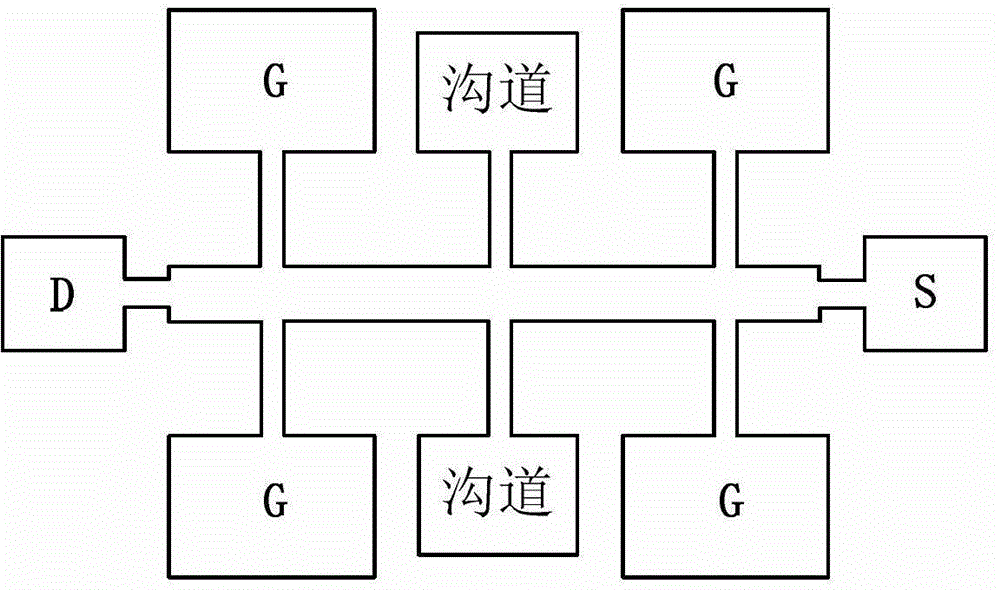
[0050] Example 1, making a connected side-gate graphene transistor.
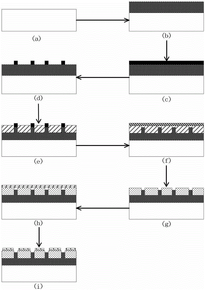
[0051] refer to figure 2 with image 3 , the manufacturing steps of this embodiment are as follows:
[0052] Step 1: Remove sample surface contaminants such as figure 2 (a).
[0053] (1.1) Clean the surface of the 4-inch Si substrate with NH 4 OH+H 2 o 2 Soak the sample in the reagent for 10 minutes, take it out and dry it to remove the organic residue on the surface of the sample;
[0054] (1.2) Use HCl+H 2 o 2 The reagent soaked the sample for 10 minutes, took it out and dried it to remove ionic contamination.
[0055] Step 2: growing the carbonized layer.
[0056] (2.1) Put the Si substrate into the reaction chamber of the CVD system, and evacuate the reaction chamber to 10 -7 mbar level;
[0057] (2.2) in H 2 In the case of protection, the temperature of the reaction chamber is raised to the carbonization temperature of 1000 ° C, and then the flow rate of 40 sccm is introduced into the rea...
Embodiment 2
[0089] Embodiment 2, making a non-connected side-gate graphene transistor.
[0090] refer to Figure 4 with Figure 5 , the implementation steps of this embodiment are as follows:
[0091] Step 1: Clean the surface of the 12-inch Si substrate, that is, use NH 4 OH+H 2 o 2 Soak the sample in the reagent for 10 minutes, take it out and dry it to remove the organic residue on the surface of the sample; then use HCl+H 2 o 2 Soak the sample in the reagent for 10 minutes, take it out and dry it to remove ionic contaminants such as Figure 4 (a).
[0092] Step 2: growing a carbonized layer. Put the Si substrate substrate into the reaction chamber of the CVD system, and evacuate the reaction chamber to 10 -7 mbar level; then in H 2 In the case of protection, the temperature of the reaction chamber is raised to the carbonization temperature of 1150 ° C, and then the flow rate of 40 sccm is introduced into the reaction chamber. 3 h 8 , and continued for 8min to grow a carbon...
Embodiment 3
[0117] Example 3, making a connected side-gate graphene transistor.
[0118] refer to figure 2 with image 3 , the implementation steps of this embodiment are as follows:
[0119] Step A: Remove sample surface contaminants such as figure 2 (a).
[0120] (A1) Clean the surface of the 8-inch Si substrate, that is, use NH 4 OH+H 2 o 2 Soak the sample in the reagent for 10 minutes, take it out and dry it to remove the organic residue on the surface of the sample;
[0121] (A2) Use HCl+H 2 o 2 The reagent soaked the sample for 10 minutes, took it out and dried it to remove ionic contamination.
[0122] Step B: growing a carbonized layer.
[0123] (B1) Put the Si substrate into the reaction chamber of the CVD system, and evacuate the reaction chamber to 10 -7 mbar level;
[0124] (B2) in H 2 In the case of protection, the temperature of the reaction chamber is raised to the carbonization temperature of 1050 ° C, and then the flow rate of 40 sccm is introduced into the...
PUM
| Property | Measurement | Unit |
|---|---|---|
| thickness | aaaaa | aaaaa |
| thickness | aaaaa | aaaaa |
| thickness | aaaaa | aaaaa |
Abstract
Description
Claims
Application Information
 - R&D
- Intellectual Property
- Life Sciences
- Materials
- Tech Scout
- Unparalleled Data Quality
- Higher Quality Content
- 60% Fewer Hallucinations
Browse by: Latest US Patents, China's latest patents, Technical Efficacy Thesaurus, Application Domain, Technology Topic, Popular Technical Reports.
© 2025 PatSnap. All rights reserved.Legal|Privacy policy|Modern Slavery Act Transparency Statement|Sitemap|About US| Contact US: help@patsnap.com