

Semiconductor device for expanding safety operation area
A safe working area, semiconductor technology, applied in the direction of semiconductor devices, electrical components, circuits, etc., can solve the problems of difficult realization of devices, life limit, device degradation, etc., to reduce the turn-on resistance, increase the saturation current, and reduce the surface current density. Effect
- Summary
- Abstract
- Description
- Claims
- Application Information
AI Technical Summary
Problems solved by technology
Method used
Image

Examples
no. 1 example
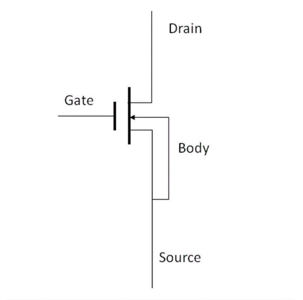
[0034] refer to Figure 2a and Figure 2b , Figure 2a The shown device includes an NMOS field effect transistor and a potential correlation circuit. The potential correlation circuit is specifically a short-circuit interconnection wire, and the body electrode Body and the gate Gate of the NMOS field effect transistor are short-circuited together, so that the body electrode Body and the gate gate are connected together. Potential of pole Gate is the same; Figure 2b The shown device includes a PMOS field effect transistor and a potential correlation circuit. The potential correlation circuit is specifically a short-circuit interconnection wire, and the body electrode Body and the gate Gate of the PMOS field effect transistor are short-circuited together, so that the body electrode Body and the gate gate are connected together. Potentials of poles and gates are the same.
[0035] exist Figure 2a and Figure 2b Under the configuration structure shown, the body electrode Bo...
no. 2 example
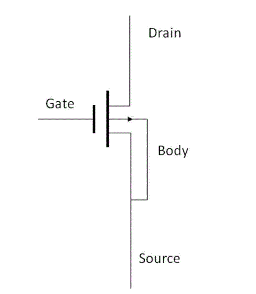
[0038] refer to Figure 3a and Figure 3b , Figure 3a The shown device includes an NMOS field effect transistor and a potential correlation circuit. The potential correlation circuit specifically includes one or more resistors 30 connected in series. The body electrode Body of the NMOS field effect transistor is connected to the gate Gate via the resistor 30, so that the body electrode Body The potential of is associated with the potential of the gate Gate; Figure 2b The shown device includes a PMOS field effect transistor and a potential correlation circuit. The potential correlation circuit specifically includes one or more resistors 30 connected in series. The body electrode Body of the PMOS field effect transistor is connected to the gate Gate via the resistor 30, so that the body electrode Body The potential of is related to the potential of the gate Gate.
[0039] exist Figure 3a and Figure 3bUnder the configuration structure shown, the body electrode Body and t...
no. 3 example
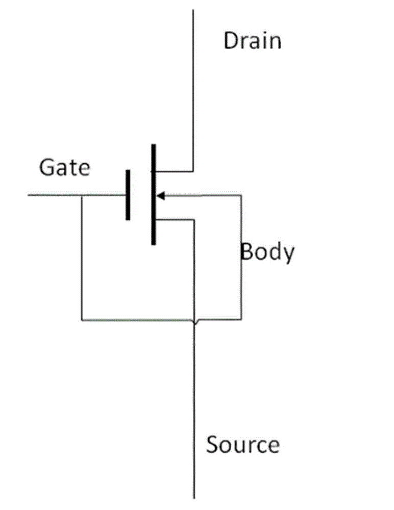
[0043] refer to Figure 4a , Figure 4a The shown device includes an NMOS field effect transistor and a potential correlation circuit, and the potential correlation circuit specifically includes one or more diodes 40 connected in series, and the body electrode Body of the NMOS field effect transistor is connected to the gate Gate Gate The body electrode Body is connected to the cathode of the diode 40, and the gate electrode Gate is connected to the anode of the diode 40, so that the potential of the body electrode Body is correlated with the potential of the gate Gate.
[0044] refer to Figure 4b , Figure 4b The shown device includes a PMOS field effect transistor and a potential correlation circuit. The potential correlation circuit specifically includes one or more diodes 40 connected in series. The body electrode Body is connected to the anode of the diode 40, and the gate electrode Gate is connected to the cathode of the diode 40, so that the potential of the body el...
PUM
 Abstract
Description
Claims
Application Information