Method for preparing cadmium telluride semiconductor thin film by electrochemical deposition
An electrochemical and cadmium telluride technology, which is applied in the field of electrochemical deposition to prepare cadmium telluride semiconductor thin films, can solve the problems of slow deposition rate, slow preparation rate, and increased time consumption, and achieve improved production efficiency, good crystallinity, and low cost. cheap effect
- Summary
- Abstract
- Description
- Claims
- Application Information
AI Technical Summary
Problems solved by technology
Method used
Image

Examples
Embodiment 1
[0033] A method for preparing a cadmium telluride semiconductor thin film by electrochemical deposition, comprising the following four steps:
[0034] 1) Preparation of CdTe alkaline precursor deposition solution: according to 0.0001 ~ 0.5mol / L tellurium dioxide (TeO 2 ), 0.005 ~ 5mol / L cadmium salt and 0.005 ~ 0.5mol / L complexing agent were put into a large beaker filled with deionized water, and the TeO 2 , cadmium sulfate and complexing agent are all dissolved, adjust the pH to 9.0 with KOH, and set aside;
[0035] 2) Cleaning and treatment of the deposition substrate: ultrasonically clean the required deposition substrate with acetone, absolute ethanol, and deionized water for 15 minutes each, transfer to the rapid retreat treatment, and cool down for later use;
[0036] 3) Electrochemical deposition of CdTe thin film: put the deposition substrate in the alkaline precursor deposition solution prepared in step 1), irradiate with a light source, deposit at a temperature of ...
Embodiment 2
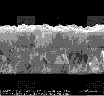
[0040] A method for preparing a cadmium telluride semiconductor thin film by electrochemical deposition, the steps are the same as in Example 1, wherein: step 1) adjust the pH to 9.0, and step 3) under the light of 15mW / cm 2 , deposited at a temperature of 40°C and a cathode potential of -0.8V, and the deposition time was 60min. The cross-sectional view of the prepared cadmium telluride semiconductor thin film is shown in image 3 .
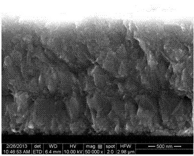
[0041] Figure 4 It is a cross-sectional view of a cadmium telluride semiconductor thin film prepared under the condition of no light, and other preparation methods and parameters are the same as image 3 same.
[0042] from image 3 and Figure 4 It can be seen that the cadmium telluride semiconductor thin film prepared under the condition of light is very thick, very dense and has very good crystallinity.
Embodiment 3
[0044] A method for preparing a cadmium telluride semiconductor thin film by electrochemical deposition, the steps are the same as in Example 2, except that the light in step 3) is 15mW / cm 2 . The cross-sectional view of the prepared cadmium telluride semiconductor thin film is shown in Figure 5 .
[0045] and in Example 2 Figure 4 In comparison, the cadmium telluride semiconductor thin film prepared under the enhanced light intensity in this embodiment is very thick.
PUM
 Abstract
Description
Claims
Application Information
PatSnap Eureka turns technology decisions into work you can execute. Powered by our Innovation Knowledge Graph, it runs expert workflows across engineering, life sciences, materials and intellectual property. Get your review-ready output in minutes.


