Insulated gate bipolar transistor (IGBT) and producing method thereof

The technology of a bipolar transistor and a manufacturing method is applied in the manufacture of insulated gate bipolar transistors and the field of insulated gate bipolar transistors, which can solve the problems of high base resistance, large Joule heat, large on-state voltage, etc., so as to reduce conduction Resistance, the effect of reducing resistance and Joule heating, increasing current density

Active Publication Date: 2013-06-26
SHANGHAI HUAHONG GRACE SEMICON MFG CORP
View PDF4 Cites 2 Cited by
  • Summary
  • Abstract
  • Description
  • Claims
  • Application Information

AI Technical Summary

Problems solved by technology

Although increasing the thickness of the drift region 101 can improve the withstand voltage capability of the device, at the same time, the base resistance of the device will be higher, the Joule heat will be larger during the on-state, and the on-state voltage will be larger during operation.

Method used


Image

  • Insulated gate bipolar transistor (IGBT) and producing method thereof
  • Insulated gate bipolar transistor (IGBT) and producing method thereof
  • Insulated gate bipolar transistor (IGBT) and producing method thereof

Examples


Embodiment Construction

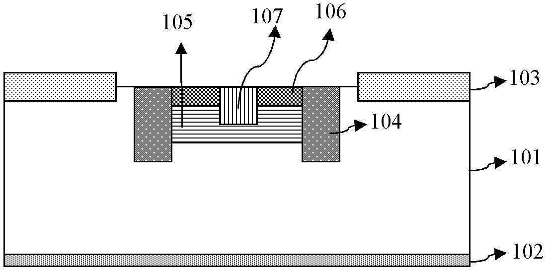
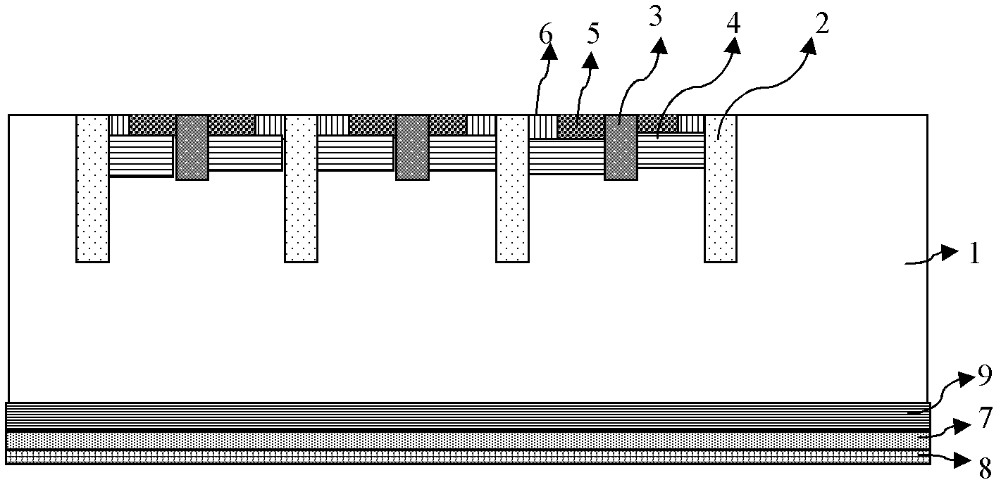
[0039] Such as figure 2 Shown is a schematic diagram of the structure of the IGBT of the embodiment of the present invention; the insulated gate bipolar transistor of the embodiment of the present invention includes:

[0040] The collector region 7 is composed of a P-type layer formed at the bottom of the silicon substrate, and the back metal 8 is formed from the back of the silicon substrate to lead out the collector.

[0041] The field stop layer 9 is composed of an N-type injection layer formed on the bottom of the silicon substrate, and the N-type injection layer is located on the upper part of the collector region and is in contact with the collector region.

[0042] The drift region 1 is composed of a first N-type layer formed in the silicon substrate, the first N-type layer is located on the N-type implanted layer, and the doping concentration of the N-type implanted layer is greater than that of the Doping concentration of the first N-type layer. The thickness of th...


PUM


Abstract

The invention discloses an IGBT and a producing method thereof. The IGBT comprises a plurality of P-type columns which divide a drift region into a plurality of units, first N-type layers between the P-type columns form a structure in which P-type thin layers and N-type thin layers are arranged alternately, so that an N-channel metal oxide semiconductor (NMOS) forming an IGBT device is in a super-junction MOS structure; as the super-junction MOS structure enables drift region of the device to be used up easily, the voltage endurance capacity of the drift region and the overall voltage endurance capacity of the device can be improved; and the dosage concentration of the drift region can be improved and the thickness of the drift region can be reduced due to improvement of the voltage endurance capacity of the drift region, so that the conducting resistance of the device can be reduced, the current density of the device can be increased, the on-state resistance and joule heat of the device can be reduced, and the turn-off response speed of the device can be improved.

Description

technical field [0001] The invention relates to the field of manufacturing semiconductor integrated circuits, in particular to an insulated gate bipolar transistor, and also relates to a manufacturing method of the insulated gate bipolar transistor. Background technique [0002] Insulated Gate Bipolar Transistor (IGBT) is a voltage-controlled MOS / bipolar composite device, which has the main advantages of both bipolar junction power transistors and power MOSFETs: high input impedance, input Small driving power, small on-resistance, large current capacity, fast switching speed, etc. The IGBT structure is very similar to the VDMOS structure, such as figure 1 As shown, it is a schematic diagram of the structure of the existing IGBT, including: the collector region 102 is composed of a P-type layer formed at the bottom of the silicon substrate, and the collector is drawn from the back of the silicon substrate; the drift region 101 is formed on the The N-type layer in the silico...

Claims


Application Information

Patent Timeline
Patent Type & Authority Applications(China)
IPC IPC(8): H01L29/739H01L29/06H01L21/331
Inventor 王海军李江华
Owner SHANGHAI HUAHONG GRACE SEMICON MFG CORP
Why Eureka
Try Eureka