Semiconductor structure, formation method of semiconductor structure, complementary metal-oxide-semiconductor transistor (CMOS) and formation method of CMOS

A semiconductor and stress technology, applied in semiconductor devices, semiconductor/solid-state device manufacturing, transistors, etc., to reduce leakage current, improve electrical performance, and improve leakage current phenomenon

Active Publication Date: 2013-07-03
SEMICON MFG INT (SHANGHAI) CORP
View PDF6 Cites 7 Cited by
  • Summary
  • Abstract
  • Description
  • Claims
  • Application Information

AI Technical Summary

Problems solved by technology

[0004] However, the existing fin field effect t

Method used


Image

  • Semiconductor structure, formation method of semiconductor structure, complementary metal-oxide-semiconductor transistor (CMOS) and formation method of CMOS
  • Semiconductor structure, formation method of semiconductor structure, complementary metal-oxide-semiconductor transistor (CMOS) and formation method of CMOS
  • Semiconductor structure, formation method of semiconductor structure, complementary metal-oxide-semiconductor transistor (CMOS) and formation method of CMOS

Examples


Embodiment Construction

[0059] It can be seen from the background technology that the existing fin field effect transistor has a serious leakage current phenomenon. In this regard, the inventors of the present invention have studied the fin field effect transistor forming process and found that the fin field effect transistor of the prior art The fin formation process of the transistor is:

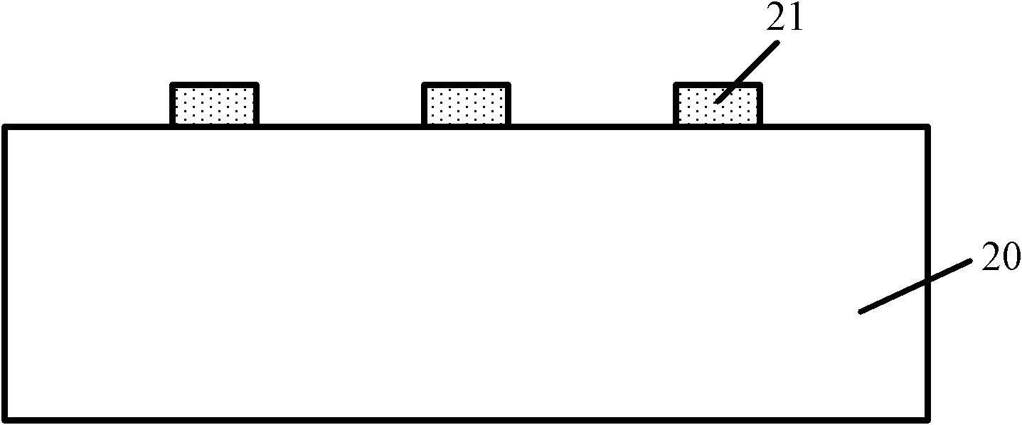
[0060] Please refer to figure 2 , a substrate 20 is provided, and a patterned photoresist layer 21 is formed on the surface of the substrate 20 .

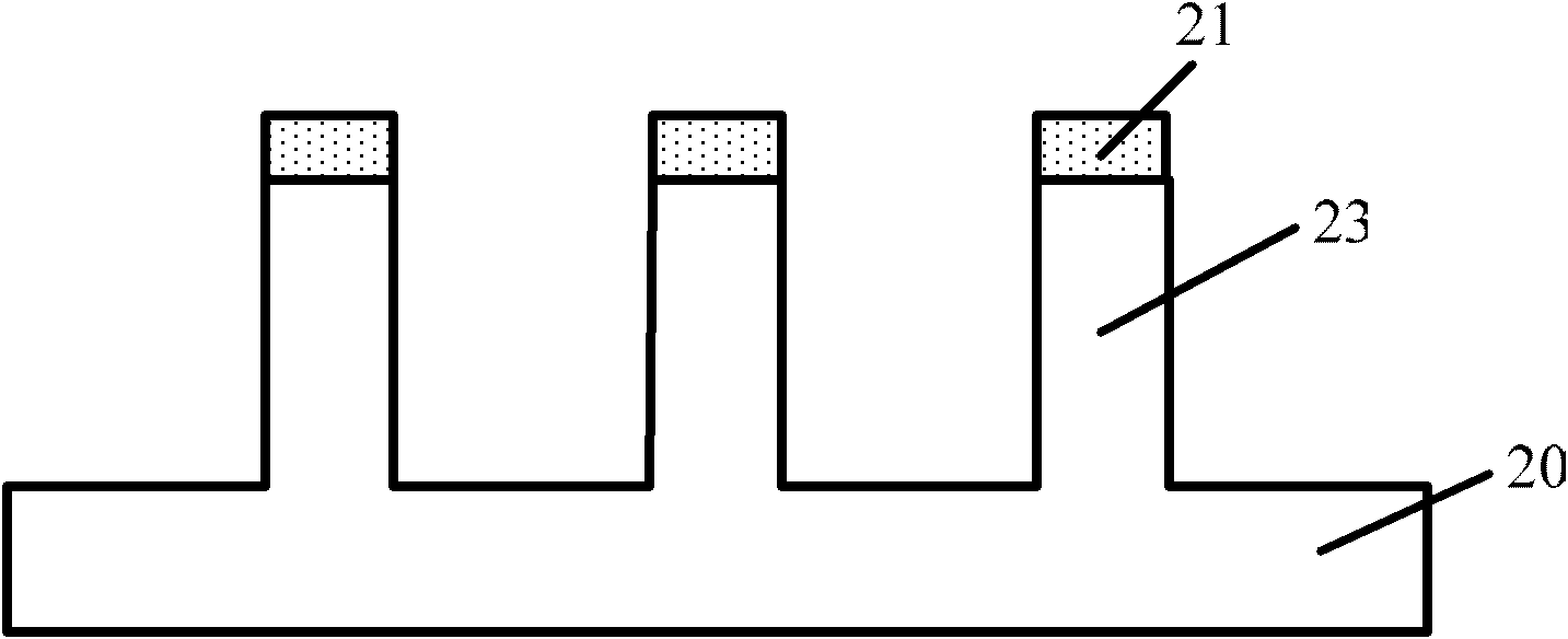
[0061] Please refer to image 3 , using the patterned photoresist layer 21 as a mask to etch the base 20 to form protruding fins 23 .

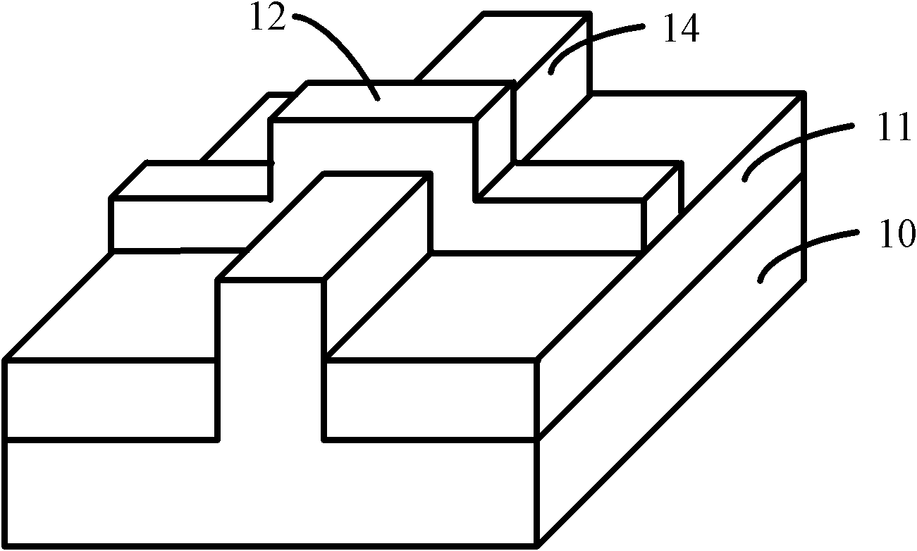
[0062] Afterwards, the inventors of the present invention formed fin field effect transistors using the fins formed by the above forming process (please refer to figure 1 ), and researched the leakage current phenomenon of fin field effect transistors, it was found that: the fins of the existing fin field effect transistors are ob...


PUM

PropertyMeasurementUnit
Stressaaaaaaaaaa
Stressaaaaaaaaaa

Abstract

The invention discloses a semiconductor structure, a formation method of the semiconductor structure, a complementary metal-oxide-semiconductor transistor (CMOS) and a formation method of CMOS. The semiconductor structure comprises a semiconductor substrate, first side stress walls and second side stress walls, wherein a fin part is arranged on the surface of the semiconductor substrate, the first side stress walls are positioned on the surface of the semiconductor substrate and on the two sides of the bottom of the fin part, the second side stress walls are positioned on the two sides of the top of the fin part, and the stress types of the first side stress walls and the second side stress walls are contrary. The electrical properties of the semiconductor structure and the CMOS are good, and the technological windows of the semiconductor structure formation method and the CMOS formation method are large.

Description

technical field [0001] The invention relates to the field of semiconductor manufacturing, in particular to a semiconductor structure and its forming method, CMOS and its forming method. Background technique [0002] With the continuous development of semiconductor process technology and the gradual reduction of process nodes, gate-last (gate-last) process has been widely used to obtain an ideal threshold voltage and improve device performance. However, when the feature size (CD, Critical Dimension) of the device is further reduced, even if the gate-last process is adopted, the structure of the conventional MOS field effect transistor can no longer meet the requirements for device performance, and the fin field effect transistor (Fin FET) as Substitution of conventional devices has received extensive attention. [0003] figure 1 A schematic diagram of a three-dimensional structure of a fin field effect transistor in the prior art is shown. like figure 1 As shown, it inclu...

Claims


Application Information

Patent Timeline
IPC IPC(8): H01L29/423H01L29/78H01L21/28H01L27/092H01L21/8238
CPCH01L29/7843H01L21/283H01L21/31H01L21/31111H01L21/823807H01L21/823821H01L21/823828H01L21/823857H01L21/823864H01L21/845H01L27/0924H01L27/1211H01L29/66795H01L29/785
Inventor 鲍宇
Owner SEMICON MFG INT (SHANGHAI) CORP
Why Eureka
Try Eureka