

Schottky semiconductor device with super junction structure and manufacturing method thereof
A technology of semiconductor and Schottky potential, applied in the field of Schottky semiconductor devices, can solve the problems of high on-resistance, affecting the reverse breakdown characteristics of devices, etc., and achieve the effect of improving the reverse breakdown voltage
- Summary
- Abstract
- Description
- Claims
- Application Information
AI Technical Summary
Problems solved by technology
Method used
Image

Examples
Embodiment 1
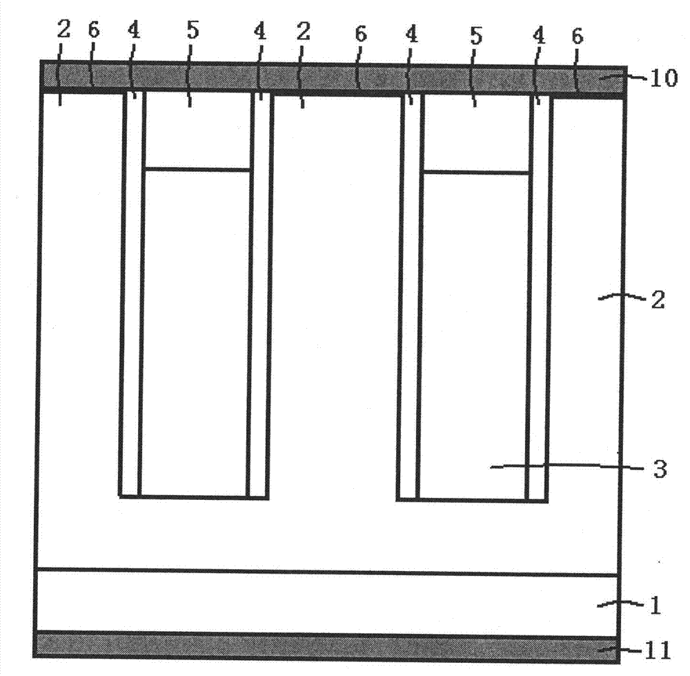
[0036] figure 1 It is a Schottky semiconductor device with a super junction structure of the present invention, combined below figure 1 The semiconductor device of the present invention will be described in detail.
[0037] A Schottky semiconductor device with a superjunction structure, comprising: a substrate layer 1, which is an N-conductivity type semiconductor silicon material, and the doping concentration of phosphorus atoms is 1E19 / CM 3 , on the lower surface of the substrate layer 1, the electrode is drawn out through the lower surface metal layer 11; the N-type semiconductor silicon material 2, located on the substrate layer 1, is an N-conduction type semiconductor silicon material, and the doping concentration of phosphorus atoms is 1E16 / CM 3 ;Lightly doped P-type semiconductor polysilicon material 3, located in the lower part of the trench, is a P-conduction type semiconductor silicon material, and the doping concentration of boron atoms is 1E16 / CM 3 ; Heavily dope...
Embodiment 2
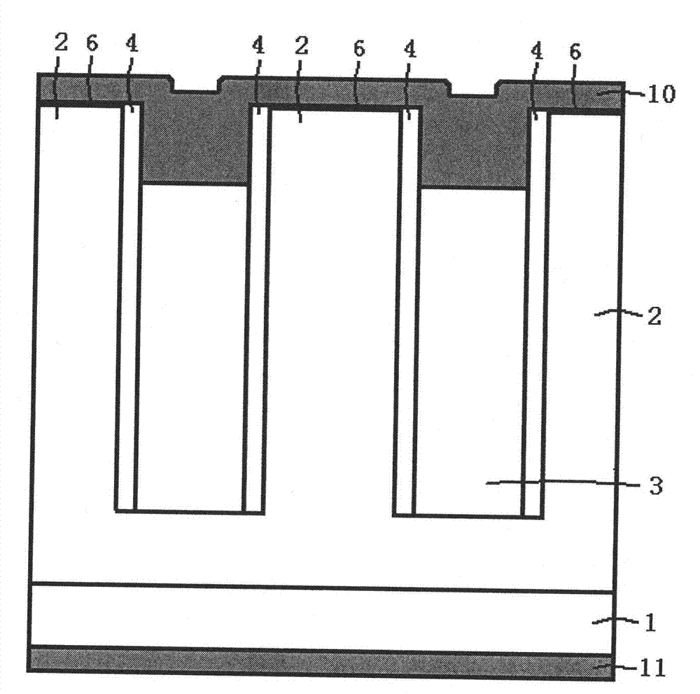
[0049] figure 2 It is a Schottky semiconductor device with a super junction structure of the present invention, combined below figure 2 The semiconductor device of the present invention will be described in detail.
[0050] A Schottky semiconductor device with a superjunction structure, comprising: a substrate layer 1, which is an N-conductivity type semiconductor silicon material, and the doping concentration of phosphorus atoms is 1E19 / CM 3 , on the lower surface of the substrate layer 1, the electrode is drawn out through the lower surface metal layer 11; the N-type semiconductor silicon material 2, located on the substrate layer 1, is an N-conduction type semiconductor silicon material, and the doping concentration of phosphorus atoms is 1E16 / CM 3 ;Lightly doped P-type semiconductor silicon material 3, located in the lower part of the trench, is a P-type semiconductor polysilicon material, and the doping concentration of boron atoms is 1E16 / CM 3 The thermal oxidation lay...
Embodiment 3
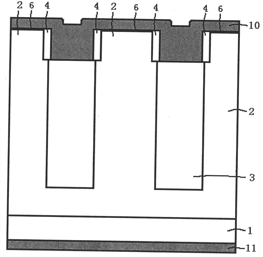
[0061] image 3 It is a Schottky semiconductor device with a super junction structure of the present invention, combined below image 3 The semiconductor device of the present invention will be described in detail.
[0062] A Schottky semiconductor device with a superjunction structure, comprising: a substrate layer 1, which is an N-conductivity type semiconductor silicon material, and the doping concentration of phosphorus atoms is 1E19 / CM 3 , on the lower surface of the substrate layer 1, the electrode is drawn out through the lower surface metal layer 11; the N-type semiconductor silicon material 2, located on the substrate layer 1, is an N-conduction type semiconductor silicon material, and the doping concentration of phosphorus atoms is 1E16 / CM 3 ;Lightly doped P-type semiconductor silicon material 3, located in the lower part of the trench, is a P-type semiconductor silicon material, and the doping concentration of boron atoms is 1E16 / CM 3 The thermal oxidation oxide l...
PUM
| Property | Measurement | Unit |
|---|---|---|
| Doping concentration | aaaaa | aaaaa |
Abstract
Description
Claims
Application Information