Bipolar resistive access memory and preparation method thereof

A technology of resistive memory and devices, which is applied in the field of resistive memory and its preparation, and can solve problems such as the performance difference of RRAM devices

Inactive Publication Date: 2013-07-10
HEBEI UNIVERSITY
View PDF1 Cites 3 Cited by
  • Summary
  • Abstract
  • Description
  • Claims
  • Application Information

AI Technical Summary

Problems solved by technology

Furthermore, in view of the wide variety of electrode materials and materials with resistance switching effects, choosi

Method used


Image

  • Bipolar resistive access memory and preparation method thereof
  • Bipolar resistive access memory and preparation method thereof
  • Bipolar resistive access memory and preparation method thereof

Examples


Embodiment 1

[0030] Example 1 Preparation of Au / ɑ-Fe 2 o 3 / FTO bipolar resistive memory device

[0031] Such as Figure 5 As shown, the preparation of α-Fe 2 o 3 The devices used for the film include: ultrasonic oscillator 1, container 2, compressed air machine 3, compressed gas control valve 4, atomizing gas control valve 5, heating device 8, and reaction furnace 9. The container 2 where the precursor liquid is placed is provided with input and output pipelines, a compressed gas control valve 4 is provided in the input pipeline, an atomized gas control valve 5 is provided on the output pipeline, and a spraying gas is provided at the port of the output pipeline. The nozzle 10 and the spray nozzle 10 are placed in the reaction furnace 9, the reaction furnace 9 is provided with a thermocouple heating device 8, the thermocouple heating device 8 is provided with a substrate table 7 for placing an insulating bottom liner, and above the reaction furnace 9 is a Vent 11.

[0032] Specific pre...

Embodiment 2

[0041] Example 2Au / ɑ-Fe 2 o 3 / FTO bipolar resistive memory device

[0042] Common containers, atomizing devices, air compressors, reaction furnaces, heating devices and spraying devices are used.

[0043] Specific preparation method:

[0044] a. Preparation of precursor solution: Dissolve iron acetylacetonate in absolute ethanol to prepare a 0.5mol / L solution as a precursor solution;

[0045] b. Place the silicon chip base substrate sprayed with fluorine-doped tin oxide film on the heating device in the reaction furnace, and heat it until the temperature in the reaction furnace rises to 350-450 ° C;

[0046] c. Place the precursor liquid in a container and atomize it through an ultrasonic atomization device. The atomized gas is transported to the reaction furnace under the action of compressed air, and sprayed onto the heated fluorine-doped tin oxide film through a nozzle, and deposited on The thickness is 30nm~100nm, forming ɑ-Fe 2 o 3 Film; the flow rate of the compre...

Embodiment 3

[0050] Embodiment 3 tests the performance of the device prepared in embodiment 1

[0051] Test instrument: Keithley4200 source test unit.

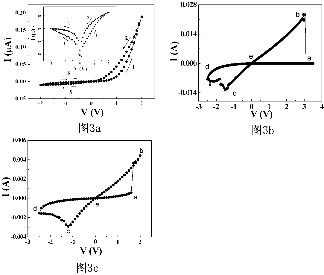
[0052] Test items: the voltage-current characteristics of the device, as well as the basic function, fatigue resistance and retention characteristics of the device.

[0053] Test Results:

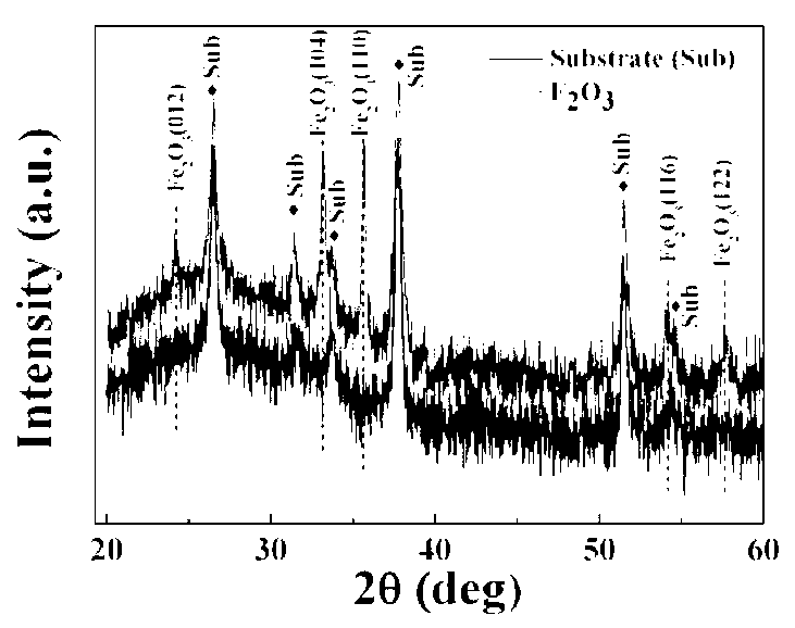
[0054] (1) The resistive switching characteristics of the storage device prepared in the present invention.

[0055] The present invention uses ɑ-Fe 2 o 3 The material is used as a resistive switch material, and the film is sandwiched between the fluorine-doped tin oxide lower electrode film and the gold (or platinum, copper) upper electrode film to form a micro-sandwich structure memory unit. When a scanning voltage higher than a certain threshold is applied on the upper electrode (the scanning voltage direction is 0→+Vmax→-Vmax→0), a certain window appears in the I-V curve of the device, showing the main characteristics of the resistive switching ...


PUM


Abstract

The invention discloses a bipolar resistive access memory and a preparation method thereof. The bipolar resistive access memory comprises an insulating substrate, an upper electrode film, a lower electrode film, wherein a resistive layer material is arranged between the upper electrode film and the lower electrode film. The bipolar resistive access memory is characterized in that the upper electrode film is a film made of one of platinum, copper or gold, the lower electrode film is a fluorine-doped tin oxide film, and the resistive layer material is an alpha-Fe2O3 polycrystalline film; and the structure of the memory is made of Pt or Cu or Au/alpha-Fe2O3/FTO. The bipolar resistive access memory has the advantages of small size, simple structure, no volatilization, quick read-write availability, low working voltage, low energy-consumption, no moving part, no destructive read out and the like.

Description

technical field [0001] The invention relates to a non-volatile memory and a preparation method thereof, in particular to a resistive variable memory and a preparation method thereof. Background technique [0002] With the rapid development of material science and semiconductor technology, various new types of non-volatile memories have also been developed rapidly. Among these new types of memory, the resistive memory device (RRAM) has attracted more and more people because of its non-volatile characteristics, high read and write speed, low power consumption, high integration, multi-valued storage capacity, and low cost. more attention. The structure of the existing RRAM is generally a "sandwich" structure, and a resistance variable layer material capable of resistance switching is provided between the upper and lower motors. Under the action of an external bias voltage, the resistance of the device will switch between high and low resistance states, thereby realizing the s...

Claims


Application Information

Patent Timeline
IPC IPC(8): H01L45/00G11C13/00
Inventor 闫小兵殷江夏奕东刘治国
Owner HEBEI UNIVERSITY
Why Eureka
Try Eureka