A kind of zinc tin nitride pn junction and preparation method thereof
A zinc tin nitride, pn junction technology, applied in the direction of final product manufacturing, sustainable manufacturing/processing, photovoltaic power generation, etc., to achieve the effect of reducing edge discharge effect, simple preparation process and low cost
- Summary
- Abstract
- Description
- Claims
- Application Information
AI Technical Summary
Problems solved by technology
Method used
Image
Examples
preparation example Construction
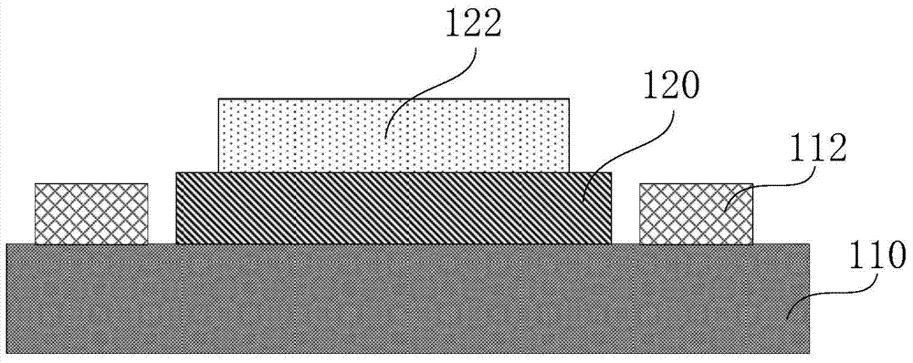
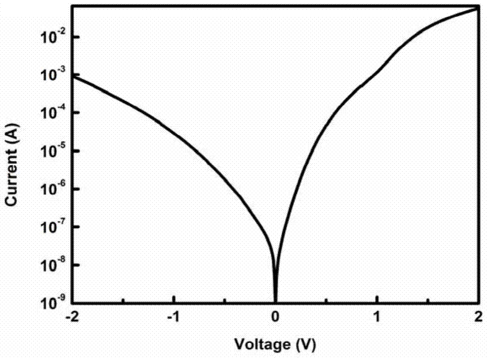
[0054] In the preparation process of the pn junction of the present invention, the n-type ZnSnN 2 If the deposition thickness of the semiconductor layer 120 is too small, the pn junction formed will have poor performance and cannot meet practical applications; if the deposition thickness is too large, it will not only increase the cost, but also be detrimental to the development trend of device miniaturization. Therefore, n-type ZnSnN 2 The thickness of the semiconductor layer 120 is preferably 60nm-300nm, within this thickness range, the obtained pn junction has obvious rectifying effect.
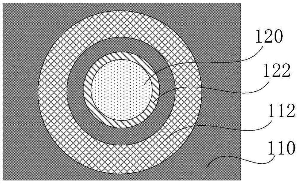
[0055] In the pn junction of the present invention, if the cross-sectional area of the electrode is too small, relatively large resistance will be generated, and the preparation is difficult; if the cross-sectional area of the electrode is too large, electric leakage will easily occur and the safety performance of the device will be reduced. Preferably, as an implementation mode, n-ty...
Embodiment 1
[0101] (1) Cut the p-type single-polished silicon wafer with ρ2 Sample silicon wafers, washed and dried;
[0102] (2) Deposit ZnSnN on p-type Si 2 . Sputtering at room temperature, set the background vacuum to 6×10 -4 Pa. The magnetron sputtering method is adopted under vacuum conditions, the sputtering power is 120W, and the working pressure is 2.0Pa. The cathode zinc-tin alloy target is bombarded with N ions, so that the target atoms are sputtered and react with N ions to form ZnSnN 2 , ZnSnN 2 The thickness is 120nm.
[0103] (3) In the sample ZnSnN 2 A layer of photoresist is spin-coated on the surface to form the first mask;
[0104] (4) Utilize the first mask of ultraviolet lithography;
[0105] (5) Corrosion of ZnSnN not protected by photoresist with etching solution 2 , to get the ZnSnN 2 The diameter of the cross-sectional circle is 100 μm.
[0106] (6) Utilize acetone and deionized water to clean the remaining photoresist in step (5);
[0107] (7) In Si-Zn...
Embodiment 2
[0112] (1) Cut the p-type single-polished silicon wafer with ρ2 Sample silicon wafers, washed and dried;
[0113] (2) Deposit ZnSnN on p-type Si 2 . Sputtering at room temperature, set the background vacuum to 6×10 -4 Pa. The magnetron sputtering method is adopted under vacuum conditions, the sputtering power is 120W, the working pressure is 2.0Pa, and the cathode zinc-tin alloy target is bombarded with N ions, so that the target atoms are sputtered and react with N ions to form ZnSnN 2 , ZnSnN 2 The thickness is 120nm.
[0114] (3) In the sample ZnSnN 2 A layer of photoresist is spin-coated on the surface to form the first mask;
[0115] (4) Utilize the first mask of ultraviolet lithography;
[0116] (5) Corrosion of ZnSnN not protected by photoresist with etching solution 2 , to get the ZnSnN 2 The diameter of the cross-sectional circle is 100 μm.
[0117] (6) Utilize acetone and deionized water to clean the remaining photoresist in step (5);
[0118] (7) In Si-Zn...
PUM
| Property | Measurement | Unit |
|---|---|---|
| thickness | aaaaa | aaaaa |
| thickness | aaaaa | aaaaa |
| diameter | aaaaa | aaaaa |
Abstract
Description
Claims
Application Information


