

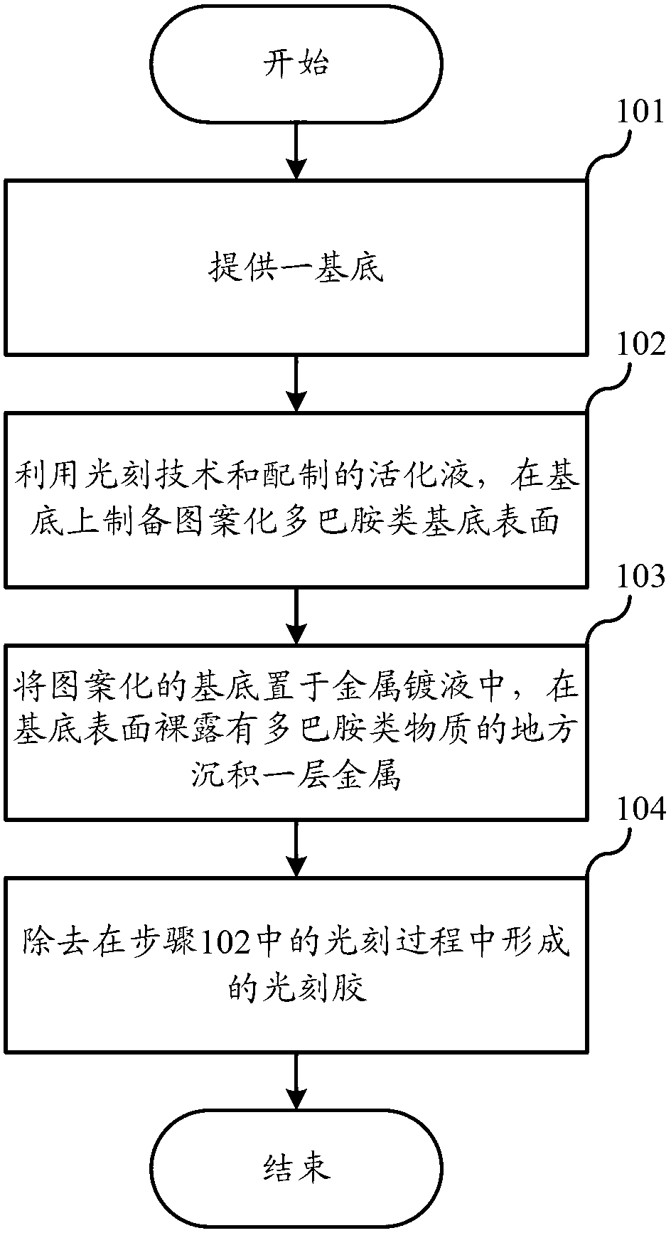
Manufacturing method of patterning metal lines
A patterned metal, patterned technology, applied in metal material coating process, circuit, liquid chemical plating, etc., can solve the problem of poor adhesion between conductive lines and substrates, unsuitable for polymer substrates, and increased surface roughness. problems, to ensure continuity and conductivity, improve surface roughness, and reduce time consumption
- Summary
- Abstract
- Description
- Claims
- Application Information
AI Technical Summary
Problems solved by technology
Method used
Image

Examples
Embodiment approach
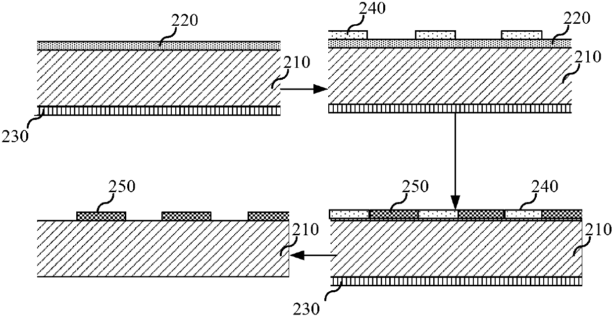
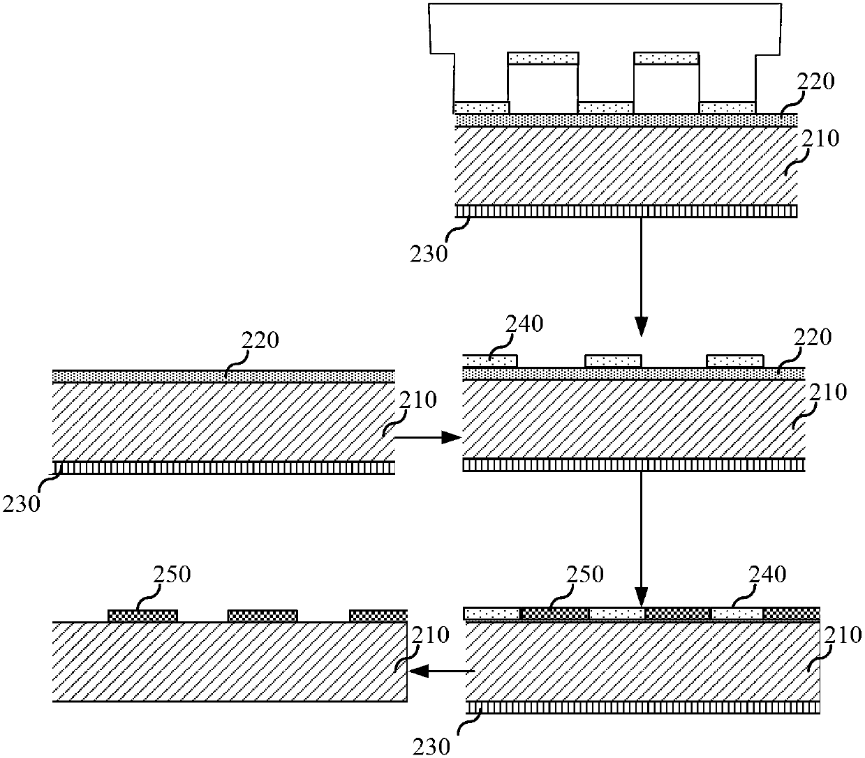
[0077] That is to say, this embodiment has the following advantages:
[0078] 1) High selectivity: metals are only deposited where dopamine exists;
[0079] 2) Wide adaptability: dopamine substances can not only deposit and adhere on hard inorganic substrates such as metal and glass, but also be loaded on substrates such as semiconductors and polymers;
[0080] 3) There is a layer of dopamine substances with excellent adhesion properties between the coating and the substrate, the binding force is better than the general method, and the metal coating does not fall off under ultrasonic conditions;
[0081] 4) All processes can be carried out at room temperature, and the time is short;
[0082] 5) The thickness of the coating can be adjusted from nanometers to micrometers, and the sheet resistance is small;
[0083] 6) After the film is bent, the film resistivity changes little;
[0084] 7) It is possible to make circuits on both sides of the substrate at the same time;
[00...
PUM
 Abstract
Description
Claims
Application Information