Large-size graphene stack structure wafer and preparation method thereof

A stacked structure and graphene technology, which is applied in semiconductor/solid-state device manufacturing, electrical components, circuits, etc., can solve the problems of fragile structures and impractical device production, and achieve the effect of improving performance

Inactive Publication Date: 2013-07-31
XIDIAN UNIV
View PDF3 Cites 10 Cited by
  • Summary
  • Abstract
  • Description
  • Claims
  • Application Information

AI Technical Summary

Problems solved by technology

Although suspended graphene holds the record for the highest carrier mobility of room temperature semiconductor materials, its fragile structure cannot be practically used for industrial device production

Method used


Image

  • Large-size graphene stack structure wafer and preparation method thereof
  • Large-size graphene stack structure wafer and preparation method thereof

Examples


Embodiment Construction

[0024] The present invention will be further described with reference to the accompanying drawings.

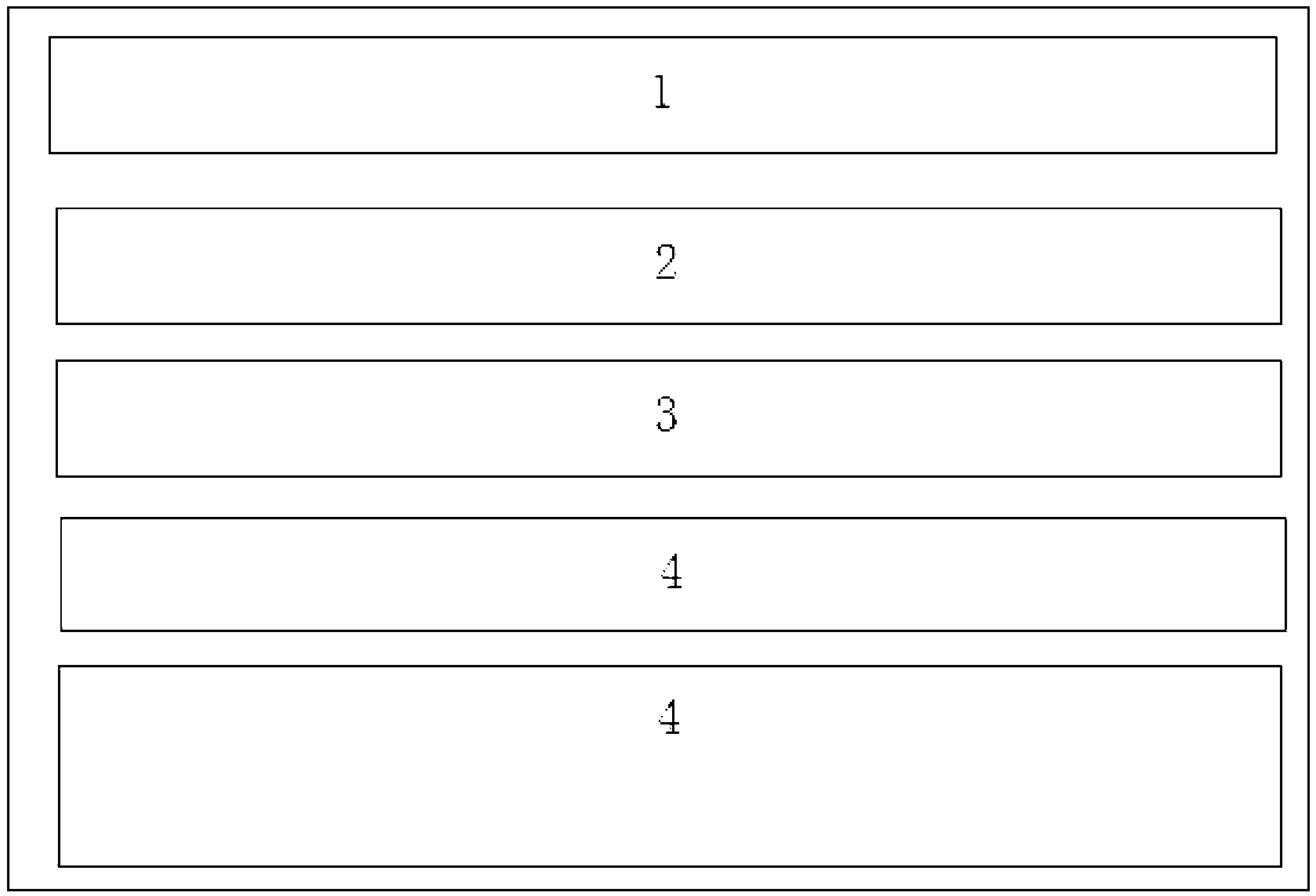
[0025] Such as figure 1 As shown, the present invention is a large-size graphene stacked structure wafer. The wafer structure from top to bottom is as follows: graphene single crystal layer 1, h-BN single crystal layer 2, and h-BN buffer layer 3. , And SiO 2 / Si wafer substrate 4.

[0026] It should be noted that the wafer size is 2 inches to 30 inches, the thickness of the graphene single crystal layer 1 is 0.335 to 4 nm, the thickness of the h-BN single crystal layer 2 is 0.6 to 50 nm, and the h- The BN buffer layer 3 has a thickness of 0.1-100 μm.

[0027] The method for preparing the foregoing large-size graphene stacked structure wafer includes the following steps:

[0028] (1) Preparation of the SiO 2 / Si wafer substrate, among them, select Si wafer, and use dry oxidation process to form SiO 2 film;

[0029] (2) Preparation of polyborazine precursor;

[0030] (3) Growing the h-BN...


PUM

PropertyMeasurementUnit
sizeaaaaaaaaaa
thicknessaaaaaaaaaa
thicknessaaaaaaaaaa

Abstract

The invention discloses a large-size graphene stack structure wafer which is characterized in that a wafer structure comprises a graphene single crystal layer, an h-BN (hexagonal boron nitride) single crystal layer, an h-BN buffer layer and SiO2/Si wafer substrates from the top down sequentially. The wafer and the preparation method have the benefits that the wafer can be compatible with a production technique of the available silicon substrate semiconductor device sufficiently, and can take full advantage of the characteristic of a hexagonal boron nitride substrate material; growing graphene has a most perfect crystal structure and a carrier transport environment with the weakest scattering; the super-high mobility of carriers in graphene is kept at the utmost; and the performance of a graphene substrate electronic device is improved greatly.

Description

Technical field [0001] The invention relates to a wafer preparation process, in particular to the structure of a large-size hexagonal boron nitride-based graphene wafer and a preparation method thereof. Background technique [0002] Graphene is an extremely excellent two-dimensional material formed by carbon atoms in a hexagonal honeycomb lattice. It has ultra-high carrier velocity and mobility, and has considerable application potential in the fields of microwave and radio frequency circuits. At present, there are three main methods for preparing graphene, namely, the mechanical peeling method, the CVD method on the catalytic metal substrate and the epitaxial growth method on the SiC substrate. Although the current experimental work on graphene electronic devices is basically based on the mechanical peeling method, the mechanical peeling method cannot prepare large-area graphene wafers. At present, many companies in the world can prepare 4-inch graphene wafers by epitaxial grow...

Claims


Application Information

Patent Timeline
Patent Type & Authority Applications(China)
IPC IPC(8): H01L29/16H01L29/20H01L21/02
Inventor 马中发张鹏吴勇庄奕琪肖郑操赵钰迪郭超冯元博
Owner XIDIAN UNIV
Why Eureka
Try Eureka