Square wave generating circuit
A square wave generating circuit and circuit technology, applied in pulse train generators and other directions, can solve the problems of long junction capacitor charging time, narrow square wave width adjustable range, large pulse width, etc., to solve the problem of falling edge delay, The effect of wide pulse adjustment range and shortened charging time
- Summary
- Abstract
- Description
- Claims
- Application Information
AI Technical Summary
Problems solved by technology
Method used
Image
Examples
Embodiment 1
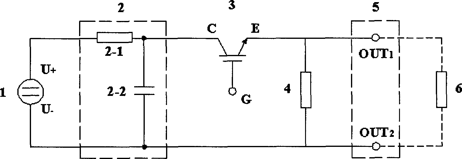
[0031] like image 3 As shown, this embodiment discloses a square wave generating circuit, including a high-voltage DC source 1, an energy storage circuit 2, a semiconductor switch 3, a charging resistor 4, and a pulse output terminal 5, and the energy storage circuit 2 includes a current limiting resistor 2-1 and the energy storage capacitor 2-2, the device under test 6 is loaded on the pulse output terminal 5; the high voltage DC source 1, the current limiting resistor 2-1 and the energy storage capacitor 2-2 form a loop, the energy storage capacitor 2-2, the semiconductor switch 3 and the device under test 6 loaded on the pulse output terminal 5 form a loop; the charging resistor 4 is connected in parallel with the pulse output terminal 5, and the charging resistor 4 is a variable resistor.
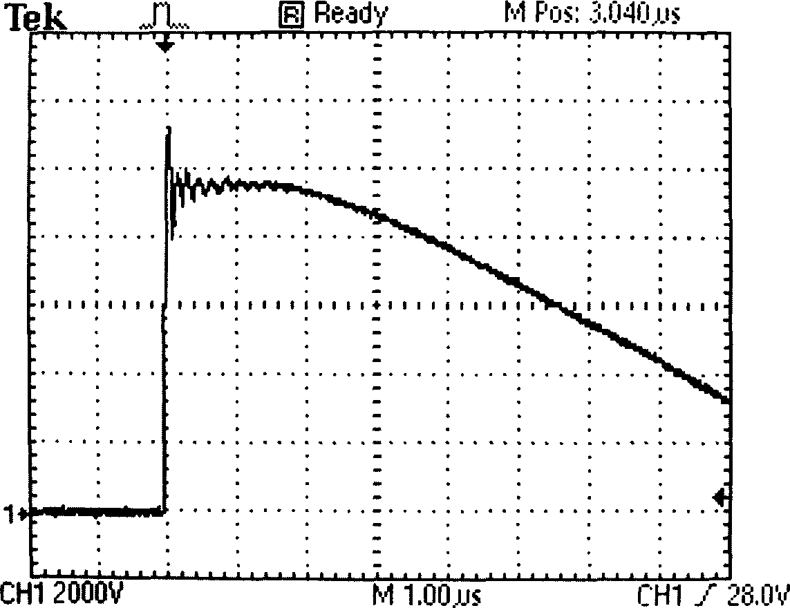
[0032] This embodiment generates square wave pulses with rising and falling edges as Figure 4 As shown, the specific working process is as follows:
[0033] The process of forming t...
Embodiment 2
[0036] like Figure 5 As shown, different from Embodiment 1, this embodiment includes a charging switch 7 and an auxiliary current-limiting resistor 8, the charging switch 7 is a power relay, and is connected in series with the charging resistor 4; the auxiliary current-limiting resistor 8 is connected in series with the semiconductor switch 3, The auxiliary current-limiting resistor 8 forms a circuit with the energy storage capacitor 2-2, the semiconductor switch 3, and the charging resistor 4, where the charging resistor 4 is a fixed resistor.
[0037] Suppose the voltage across the energy storage capacitor 2-2 is U 0 , the resistance of charging resistor 4 is R 4 , the equivalent resistance of the device under test 6 is R 6 , the resistance of the auxiliary current limiting resistor 8 is R 8 , then the voltage U across the EUT 6 loaded on the pulse output 5 6 for:
[0038] U 6 = R ...
Embodiment 3
[0041] like Image 6 As shown, the difference from Embodiment 2 is that the charging resistor 4 in this embodiment is a variable resistor, and also includes an auxiliary charging resistor 9 used to limit the longest falling edge of the pulse, and the auxiliary charging resistor 9 is connected to the pulse output terminal 5 in parallel.
[0042] The resistance value of the equivalent resistance of the equipment under test 6 in this embodiment is relatively large, and the adjustment range of the charging resistor 4 is limited. The total parallel resistance of the resistor 9 is small, thereby ensuring that the charging circuit formed by the semiconductor switch 3 junction capacitance, the charging resistor 4, the auxiliary charging resistor 9 and the equivalent resistance of the device under test 6 has a small time constant and determines the output pulse The longest falling edge time, get the output pulse with a steep falling edge.
PUM
 Abstract
Description
Claims
Application Information


