Stack type baseplate structure

A stacked, substrate technology, applied in the direction of printed circuits, electrical components, sealed enclosures, etc. where non-printed electrical components are connected, it can solve the problems of non-compliance with economic costs, difficult process control, etc., to reduce circuit short circuit or abnormality , The effect of improving production efficiency and simplifying process steps

Active Publication Date: 2013-08-14
UNIVERSAL SCIENTIFIC INDUSTRIAL (SHANGHAI) CO LTD +1
View PDF4 Cites 4 Cited by
  • Summary
  • Abstract
  • Description
  • Claims
  • Application Information

AI Technical Summary

Problems solved by technology

However, due to the process of injecting the colloid 17, several more process steps are required, which is not in line with the economic cost, and the progress of the injection needs to be controlled during the injection process, and the process is not easy to control

Method used


Image

  • Stack type baseplate structure
  • Stack type baseplate structure
  • Stack type baseplate structure

Examples


no. 1 example

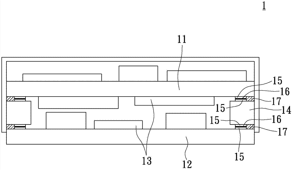
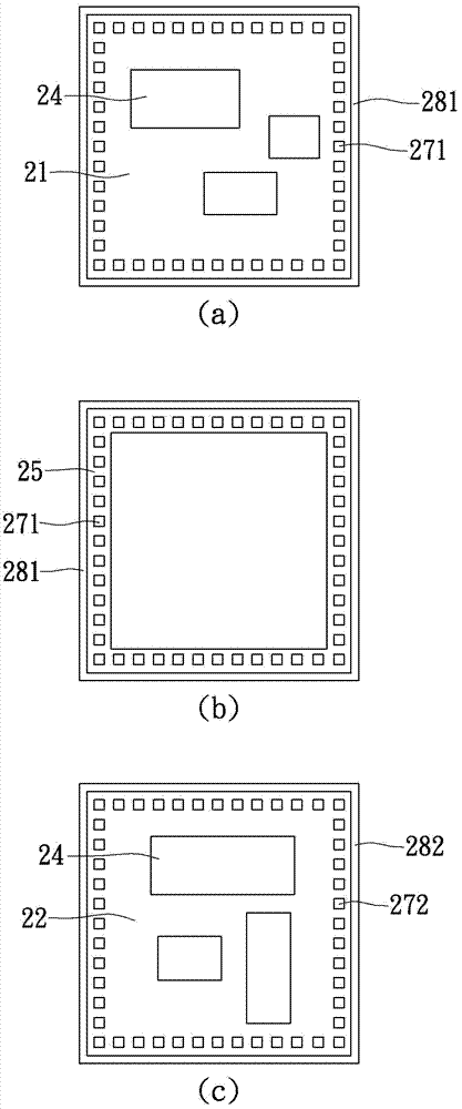
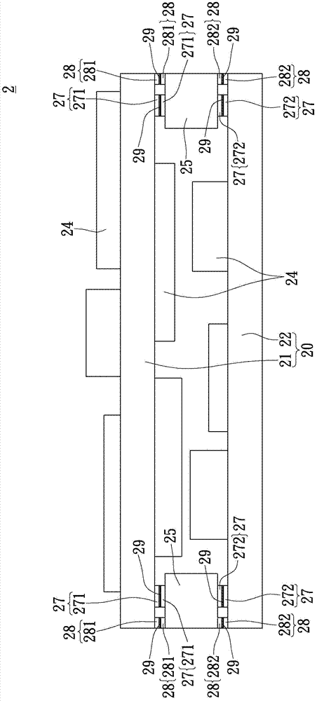
[0054] Please refer to figure 2 and image 3 As shown, a stacked substrate structure 2 includes a substrate unit 20 , a first frame 25 , a conductor unit 27 and a barrier unit 28 . First, the substrate unit 20 has a first substrate 21 and a second substrate 22, such as figure 2 Shown in (a) is the first substrate 21, figure 2 Shown in (c) is the second substrate 22, the first substrate 21 is located on the top of the second substrate 22, the first substrate 21 and the second substrate 22 respectively have a plurality of electronic components 24, the first substrate 21 and the second substrate 22 may be a printed circuit board.

[0055] Wherein, a first frame body 25 can be arranged between the first substrate 21 and the second substrate 22, such as figure 2Shown in (b) is the first frame body 25, that is to say, the first substrate 21 is stacked above the first frame body 25, and the second substrate 22 is arranged below the first frame body 25 to form a stacked struc...

no. 2 example

[0066] Please refer to Figure 7 and Figure 8 As shown, the stacked substrate structure 2 of the second embodiment can be extended from the first embodiment, that is, the structure of the first embodiment can continue to stack a layer of substrates and frames, so the bottom of the second substrate 22 can be A second frame body 26 and a third substrate 23 are provided, so that the stacked substrate structure 2 is formed by stacking three layers of substrates and two frames. Such as Figure 7 (a) is the first substrate, Figure 7 (b) shows the first frame, Figure 7 (c) is the second substrate, Figure 7 (d) is the second frame, Figure 7 (e) shows the third substrate.

[0067] Furthermore, a second conductor 272 and solder 29 can be provided on the lower side of the second substrate 22 to connect to the second frame 26, and the second frame 26 is then connected to the third substrate 23 through the third conductor 273 and solder 29. , forming a layered structure. Where...

no. 3 example

[0072] Please refer to Figure 9 and Figure 10 As shown, the stacked substrate structure 2 of the third embodiment includes a first substrate 21 , a first frame 25 , a plurality of first conductors 271 and a first barrier 281 . Such as Figure 9 (a) shows the first substrate, Figure 9 (b) shows the first frame. Firstly, the first substrate 21 can be a printed circuit board, the first frame body 25 is located on one side of the first substrate 21, the first frame body 25 can be hollow, so it can accommodate the electronic components 24 of the first substrate 21, and The first frame body 25 can have the properties of conduction and signal transmission.

[0073]Among them, a plurality of first conductors 271 are connected to the first substrate 21 and the first frame body 25, and the first conductors 271 are connected to the first conductors on the first frame body 25 through solder 29 (a metal alloy containing tin, silver or copper). The conductors 271 are electrically co...


PUM


Abstract

The invention provides a stack type baseplate structure. The stack type baseplate structure comprises a baseplate unit, a first frame body, an electric conductor unit and a blocking body unit, wherein the baseplate unit comprises a first baseplate and a second baseplate; the first frame body is arranged between the first baseplate and the second baseplate; the electric conductor unit comprises a plurality of first electric conductors and a plurality of second electric conductors; the first electric conductors are respectively connected with the first baseplate and the first frame body through soldering tin; the second electric conductors are respectively connected with the second baseplate and the first frame body through soldering tin; and the first electric conductors are electrically connected with the second electric conductors. The blocking unit comprises a first blocking body and a second blocking body, the first blocking body surrounds the first electric conductors, the second blocking body surrounds the second electric conductors, the first blocking body is closely fitted between the first baseplate and the first frame body through soldering tin, and the second blocking body is closely fitted between the second baseplate and the first frame body through soldering tin.

Description

technical field [0001] The invention relates to a substrate structure, in particular to a stacked substrate structure for printed circuit boards. Background technique [0002] With the rapid development of electronic consumer products, various electronic products according to the different needs of consumers are also constantly being introduced. In order to make general electronic products more powerful and further attract consumers' desire to buy, electronic products will gradually develop towards thinner, thinner and smaller, so the printed circuit boards used will also tend to high-density design layout, stacked multi-layer structure, and miniaturized size. , Continuously increasing functions and thin plate design. Therefore, how to fully consider the goodness of the electrical connection during the design process of the printed circuit board, and to ensure the integrity of the signal, without circuit abnormality or poor signal transmission, has become the focus of the c...

Claims


Application Information

Patent Timeline
IPC IPC(8): H05K5/06H05K9/00H05K1/18H05K3/34
Inventor 郑宗荣
Owner UNIVERSAL SCIENTIFIC INDUSTRIAL (SHANGHAI) CO LTD
Why Eureka
Try Eureka