Detecting device and method

A detection device and detection method technology, applied in the field of detection, can solve the problems of low recognition rate of liquid crystal panels, prone to false detection, low detection efficiency, etc., so as to improve the defect recognition rate and detection efficiency, improve work efficiency, and improve production automation Effect

Inactive Publication Date: 2013-08-21
HEFEI BOE OPTOELECTRONICS TECH +1
View PDF4 Cites 52 Cited by
  • Summary
  • Abstract
  • Description
  • Claims
  • Application Information

AI Technical Summary

Problems solved by technology

[0004] However, this detection method in the prior art has a low defect recognition rate for liquid crystal panels, is prone to false detection, and has low detection efficiency.

Method used


Image

  • Detecting device and method
  • Detecting device and method
  • Detecting device and method

Examples


Embodiment 1

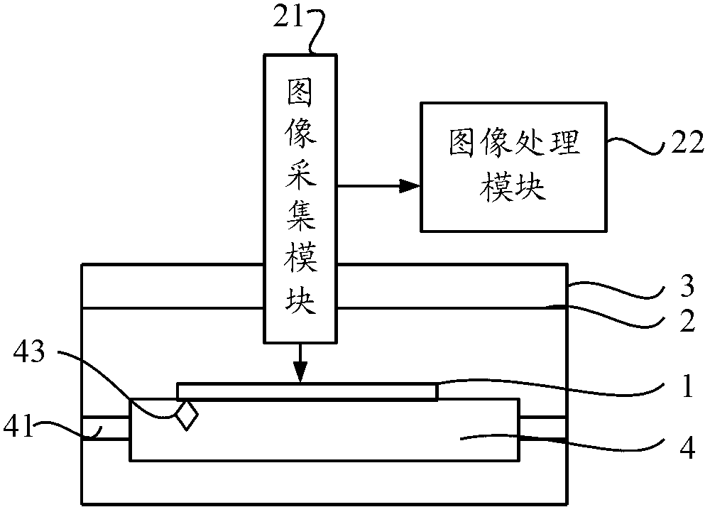
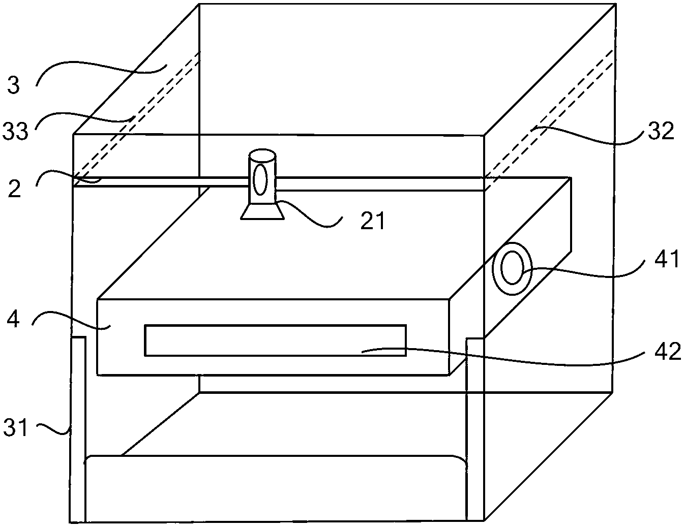
[0067] The principle schematic diagram of the detection device provided by the present invention is as follows: figure 1 As shown, the detection device includes:

[0068] An image acquisition module 21 for collecting the image information of the liquid crystal panel 1 to be tested;

[0069] The image processing module 22 is signal-connected with the image acquisition module 21. The image processing module 22 compares the received image information with the defect database to determine the defect level of the liquid crystal panel 1 to be tested.

[0070] Machine vision defect detection is based on the comparison and matching of the defect library to determine whether the defect exceeds the requirements. The defect detection needs to build the defect library of the inspected item, and quickly compare the physical object with the defect library to replace the human eye to make a qualified judgment. Defect detection requires as large an optical field of view as possible to be abl...

Embodiment 2

[0095] The present invention also provides a detection method, the flow chart of the detection method is as follows Figure 5 shown, including:

[0096] Step S501: loading the liquid crystal panel to be tested;

[0097] Step S502: the image acquisition module collects the image information of the liquid crystal panel to be tested;

[0098] Step S503: The image processing module compares the received image information with the defect database to determine the defect level of the liquid crystal panel to be tested.

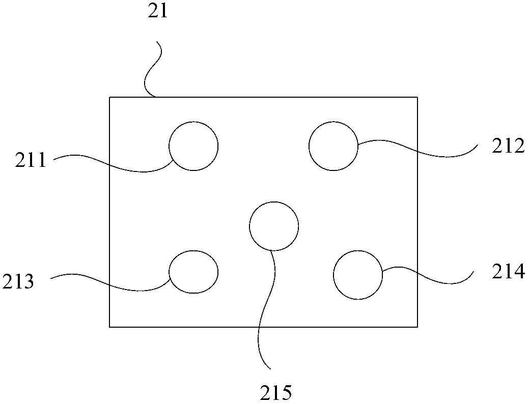
[0099] Preferably, the image acquisition module includes: a first camera tube, a second camera tube, a third camera tube, a fourth camera tube, and a fifth camera tube. Step S502: the image acquisition module collects the image information of the liquid crystal panel to be tested, which specifically includes :

[0100] Use the first camera tube to collect bad image information caused by foreign matter and / or air bubbles of the liquid crystal panel to be tested;

[...


PUM


Abstract

The invention relates to the technical field of detection, and discloses detecting device and method. The detecting device comprises an image acquiring module and an image processing module, wherein the image acquiring module acquires image information of a liquid crystal display panel to be detected, and the image processing module is in signal connection with the image acquiring module. The image processing module compares received image information with a defect database and judges defect level of the liquid crystal display panel to be detected. During use of the detecting device, the image acquiring module can acquire image information of any position of the liquid crystal display panel to be detected, the image processing module compares received the image information acquired by the image acquiring module with the defect database and judges the defect level of the liquid crystal display panel to be detected. Accordingly, by the detecting device, defect identification rate and detection efficiency of the liquid crystal display panel are improved.

Description

technical field [0001] The invention relates to the technical field of detection, in particular to a detection device and a detection method. The detection device is suitable for the detection of liquid crystal panels. Background technique [0002] With the continuous provision of liquid crystal display technology, people have higher and higher requirements for the quality and display effect of liquid crystal display products. [0003] In the production process of liquid crystal displays, it is necessary to perform defect detection on the liquid crystal panels that have been produced, so as to improve the good rate of the liquid crystal panels. Under the prior art, it is necessary to manually inspect the cell thickness of the liquid crystal panel, the alignment of the liquid crystal panel, and whether there are foreign objects in the liquid crystal panel. [0004] However, this detection method in the prior art has a low defect recognition rate for liquid crystal panels, is...

Claims


Application Information

Patent Timeline
Patent Type & Authority Applications(China)
IPC IPC(8): G02F1/13G01N21/958
CPCG09G3/36G06T7/001G06T2207/10024G06T2207/30121G09G3/006G09G2330/10G09G2360/145
Inventor 井杨坤
Owner HEFEI BOE OPTOELECTRONICS TECH
Why Eureka
Try Eureka