Microfluidic chip for sorting and application thereof

A microfluidic chip and chip technology, applied in the direction of using electricity/wave energy to treat microorganisms, specific-purpose bioreactors/fermenters, microorganisms, etc., can solve the problem of complex chip manufacturing process, repeatability to be verified, chip width Limited and other issues

Inactive Publication Date: 2013-08-28
SHANGHAI EAST HOSPITAL
View PDF3 Cites 34 Cited by
  • Summary
  • Abstract
  • Description
  • Claims
  • Application Information

AI Technical Summary

Problems solved by technology

However, the manufacturing process of this type of chip is relatively complicated, and the experimental condition control requirements are high, so the repeatability of the experiment has yet to be verified.
In 2012, Kang et al. reported a magnetic separation microfluidic chip based on a dual-channel mode. A small chamber for collecting CTCs was provided on the same side wall of two parallel microchannels, and a permanent magnet was placed outside the end of the small chamber for the microfluidic separation. A sufficiently strong magnetic field is generated in the channel. When the tumor cells labeled with magnetic beads flow through the microchannel, they will be deflected perpendicular to the direction of the flow velocity under the action of the magnetic field force and enter the collection chamber on the side wall, thereby realizing the separation of CTCs. However, the main channel width of the chip is limited, so the flow rate and sample processing capacity of the chip are low
However, the main disadvantage of this chip is that the immunomagnetic bead-labeled tumor cells attached to the cover glass by the force of the magnetic field are still subjected to strong fluid disturbance and exposed to fluid shear stress, resulting in the detachment and loss of some of the attached cells.

Method used


Image

  • Microfluidic chip for sorting and application thereof
  • Microfluidic chip for sorting and application thereof
  • Microfluidic chip for sorting and application thereof

Examples


Embodiment 1

[0136] Example 1 Microfluidic chip

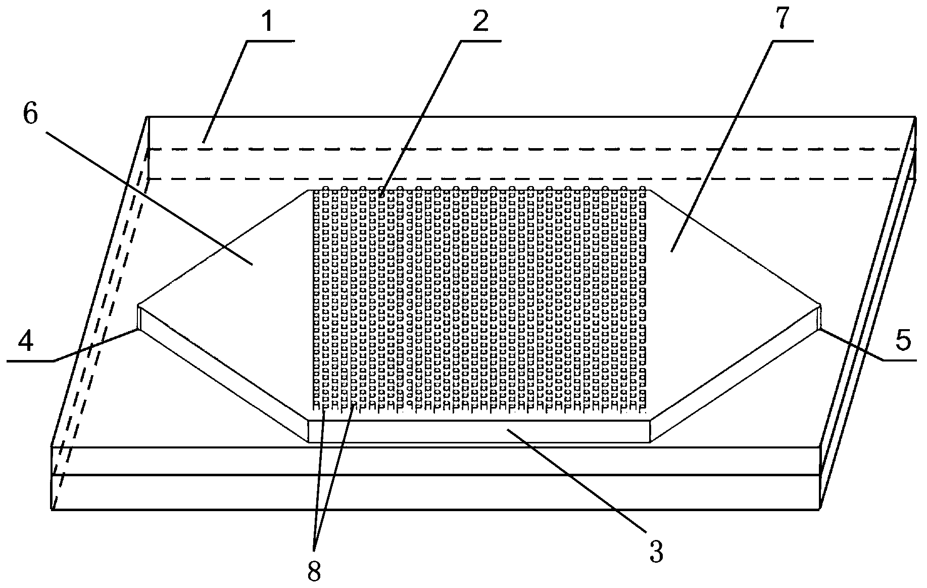
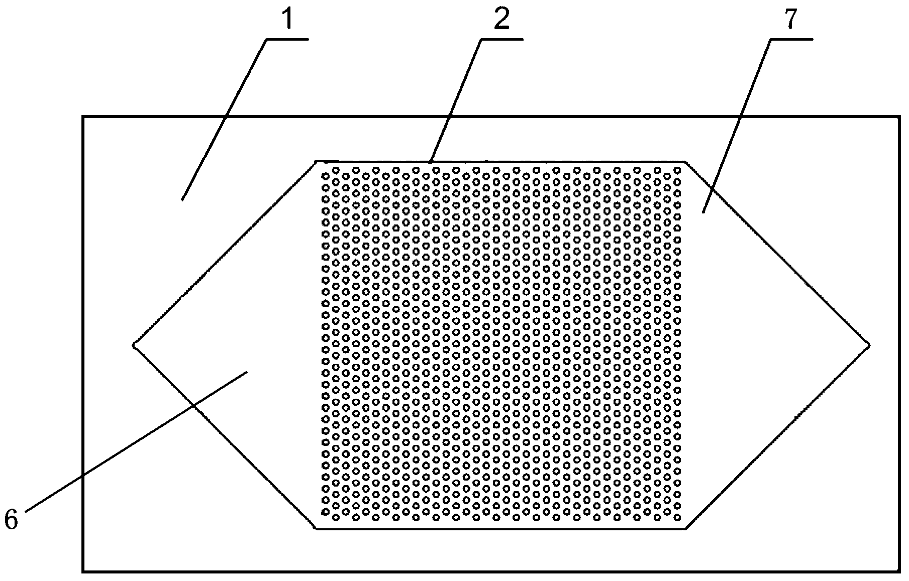
[0137] Such as Figure 1-4 As shown, the chip of the present invention is integrally formed, including:

[0138] (1) Chip inlet 4: located on the bottom surface of the microfluidic chip 1, the shape is a circle with a diameter of 500 microns, and the chip inlet 4 is connected to the main channel 3 of the chip.

[0139] (2) Main channel 3 of the chip: the main channel 3 consists of an inlet channel 6 of an isosceles right triangle with a hypotenuse length of 25.4 mm, a square capture area channel 2 with a side length of 25.4 mm, and an isosceles right angle with a hypotenuse length of 25.4 mm. A triangular exit channel 7 is formed, and the hypotenuses of the two isosceles right triangles coincide with the left and right sides of the square respectively. The chip outlet 5 and the chip inlet 4 are respectively located at the right angles of the inlet channel 6 and the outlet channel 7 of the isosceles right triangle, and the right angle of t...

Embodiment 2

[0142] Example 2 Microfluidic chip

[0143] Such as figure 1 and Figure 4 As shown, the structure of the chip in this embodiment is basically the same as that in Embodiment 1, including chip inlet, chip main channel and chip outlet. The difference is that the chip is a split structure, including a first substrate located above and a second substrate located below, and the two are closed to each other. The first substrate is provided with a collection chamber area for collecting cells or other substances to be sorted, and the collection chamber area is provided with a plurality of collection chambers with openings facing downwards, and the second substrate is provided with a chip inlet, a chip outlet, and a main channel. lower surface9. When the first substrate and the second substrate were closed, the side of the first substrate provided with the collection cell area and the main channel lower surface of the second substrate jointly formed a chip main channel for the flow ...

Embodiment 3

[0144] Example 3 Sorting of circulating tumor cells in peripheral blood of patients with colon cancer using the chip of the present invention

[0145] (1) Take 5ml of peripheral venous blood from patients with colon cancer, and remove the first 2ml of peripheral blood to avoid skin epithelial cell contamination. The remaining blood samples are collected in EDTA anticoagulant tubes, stored and transported at 4 degrees Celsius, and tested within 4 hours.

[0146] (2) Flush the channel of the microfluidic chip with block polyether F-108 for 30 minutes to prevent non-specific cell adhesion, and then place a permanent magnet with a magnetic field strength of 500mT above the capture area of ​​the microfluidic chip.

[0147] (3) According to 10 7 For the ratio of magnetic beads / ml blood, add 150 microliters of immunomagnetic beads conjugated with anti-human epithelial cell adhesion molecule antibody (purchased from Invitrogen) to 3 ml of blood in step (1), and incubate at 4°C 30 min...


PUM

PropertyMeasurementUnit
heightaaaaaaaaaa
widthaaaaaaaaaa
thicknessaaaaaaaaaa

Abstract

The invention relates to a microfluidic chip for sorting and an application thereof, and in particular discloses a microfluidic chip for sorting. The chip comprises a chip inlet, a main channel and a chip outlet, wherein the chip inlet is used for a liquid to be sorted to flow in; the main channel is used for the liquid to be sorted to flow; the chip outlet is used for discharging the sorted liquid; the main channel includes an inlet channel, an outlet channel and a capturing area channel, wherein the inlet channel is positioned on the chip inlet, the outlet channel is positioned on the chip outlet, and the capturing area channel is positioned between the inlet channel and the outlet channel; and a plurality of small collecting rooms which are provided with downward openings and used for collecting target materials to be sorted are formed in the capturing area channel. In addition, the invention further provides a microfluidic chip device and a microfluidic chip kit for sorting and a method for sorting target cells or other substances. The microfluidic chip disclosed by the invention has the advantages of simplicity in manufacturing and good operability and repeatability, the area of a cell sorting area is greatly increased, and the high-flow cell sorting is supported.

Description

technical field [0001] The invention relates to the technical field of microfluidic chips, in particular to a sorting microfluidic chip, a microfluidic chip device, a microfluidic chip kit, and a sorting method for sorting objects. Background technique [0002] Microfluidic chip technology, also known as lab-on-a-chip (lab-on-a-chip), is a micro-machining technology proposed by Swiss researchers in the 1990s to separate and sample components involved in biochemical reactions. The basic steps such as, reaction and detection are integrated on a chip with an area of ​​about several square centimeters, and the whole process is precisely controlled. The microchannels inside the chip form a controllable microfluidic network, which can be used to replace conventional biochemical detection, and has shown great development in the fields of medicine and life sciences with its characteristics of miniaturization, integration, high throughput and high precision potential and application...

Claims


Application Information

Patent Timeline
Patent Type & Authority Applications(China)
IPC IPC(8): C12M1/00C12M1/42C12N5/00C12N5/09C12N13/00C12N15/10C07K1/14
Inventor 张振宇葛海燕印晓伟代镇岭李书恒李淑萍
Owner SHANGHAI EAST HOSPITAL
Why Eureka
Try Eureka