High-voltage LED chip with microstructural antireflection film

A technology of LED chips and anti-reflection coatings, which is applied in the direction of electrical components, electrical solid devices, circuits, etc., to achieve the effects of increasing output energy, improving light output efficiency, and reducing reflection loss

Inactive Publication Date: 2013-08-28
SOUTH CHINA UNIV OF TECH
View PDF4 Cites 6 Cited by
  • Summary
  • Abstract
  • Description
  • Claims
  • Application Information

AI Technical Summary

Problems solved by technology

Therefore, the former two are not anti-reflection coating materials with better transmission properties

Method used


Image

  • High-voltage LED chip with microstructural antireflection film
  • High-voltage LED chip with microstructural antireflection film
  • High-voltage LED chip with microstructural antireflection film

Examples


Embodiment Construction

[0023] The specific implementation of the present invention will be further described below in conjunction with the accompanying drawings and examples, but the implementation and protection of the present invention are not limited thereto.

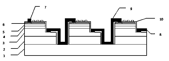
[0024] See figure 1 , a high-voltage LED chip with a microstructure anti-reflection film, including a plurality of light-emitting units, each light-emitting unit sequentially includes a gem substrate 1, a buffer layer 2, an N-type layer 3, a quantum well layer 4, a P-type Layer 5 and ITO layer 6, each light-emitting unit also includes an electrode 7 on the P-type layer and an electrode 8 on the N-type layer, and the electrodes between adjacent light-emitting units are connected by a connecting bridge 9, and each light-emitting unit also includes a covering On the anti-reflection film 10 on the ITO layer, the top surface of the anti-reflection film above the ITO layer 6 has a cylindrical microstructure.

[0025] Generally, the main lumines...


PUM


Abstract

The invention belongs to the field of semiconductor emitting device manufacturing, and particularly relates to a high-voltage LED chip with a microstructural antireflection film. The high-voltage LED chip with the microstructural antireflection film comprises a sapphire substrate, a buffering layer, a N-type layer, a quantum well layer, a P-type layer, an electrode on the P-type layer, an electrode on the N-type layer, a cross structure, an ITO layer and an antireflection film body, wherein the antireflection film body covers the ITO layer and is provided with a cylindrical microstructure. The high-voltage LED chip with the microstructural antireflection film can effectively reduce reflection losses when an LED emerges light, and meanwhile light ray total reflection from the chip to the air can be reduced through the microstructure. Meanwhile, the antireflection film can restrain dampness of the chip and diffusion of impurities, and a final protective function is achieved.

Description

technical field [0001] The invention belongs to the field of manufacturing semiconductor light-emitting devices, and in particular relates to a high-voltage LED chip with a microstructure anti-reflection film. Background technique [0002] LED is an energy-saving, environmentally friendly, long-life, and pollution-free light-emitting device. Its energy consumption is only 10% of incandescent lamps and 50% of fluorescent lamps. The luminous efficiency of the existing known high-power LEDs can reach 160lm / w, the stable working environment is a DC current of 350mA, and the working voltage is generally 3V, which cannot be directly driven by commercial power. In order to overcome the above-mentioned technical problems, high-voltage LEDs emerged as a new type of LED structure. The driving current of the high-voltage LED is generally 20mA, and the working voltage is generally 45-50V. Generally, 4 high-voltage LEDs are directly connected in series to reach the working voltage of 2...

Claims


Application Information

Patent Timeline
Patent Type & Authority Applications(China)
IPC IPC(8): H01L27/15H01L33/44
Inventor 王洪钟炯生黄华茂吴跃锋
Owner SOUTH CHINA UNIV OF TECH
Why Eureka
Try Eureka