p-type graphene film/n-type Ge schottky junction near-infrared photoelectric detector and preparation method thereof

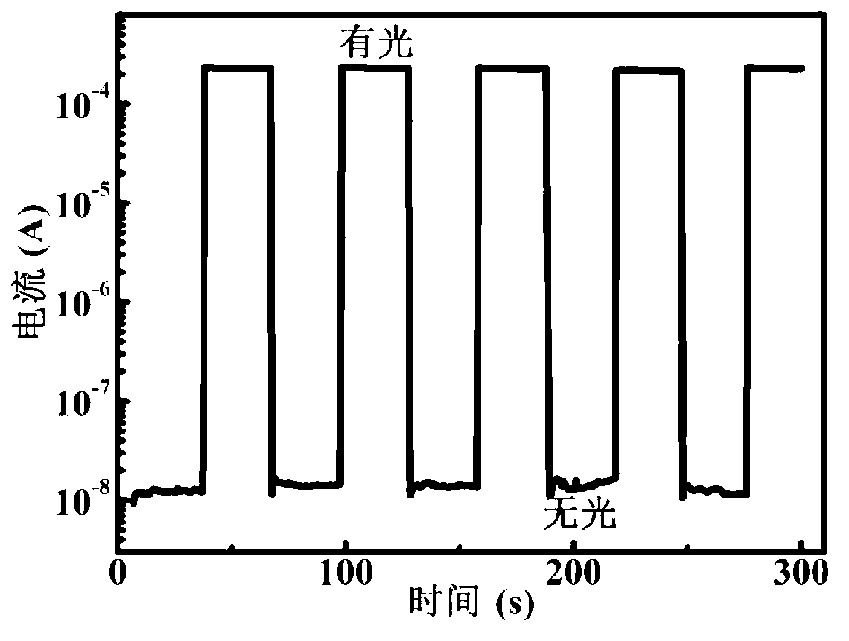
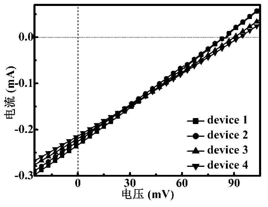
A graphene film and electrical detector technology, applied in circuits, electrical components, semiconductor devices, etc., can solve the problems of mid-infrared photodetectors that have not been reported, and achieve the effects of large switching ratio, fast response speed, and environmental protection.

Inactive Publication Date: 2013-09-04
HEFEI UNIV OF TECH
View PDF0 Cites 35 Cited by
  • Summary
  • Abstract
  • Description
  • Claims
  • Application Information

AI Technical Summary

Problems solved by technology

[0006] If graphene and germanium are combined to prepare near-infrared photodetectors, the sensitivity of germanium to near-infrared light can be used, and the excellent properties

Method used


Image

  • p-type graphene film/n-type Ge schottky junction near-infrared photoelectric detector and preparation method thereof
  • p-type graphene film/n-type Ge schottky junction near-infrared photoelectric detector and preparation method thereof
  • p-type graphene film/n-type Ge schottky junction near-infrared photoelectric detector and preparation method thereof

Examples


Embodiment 1

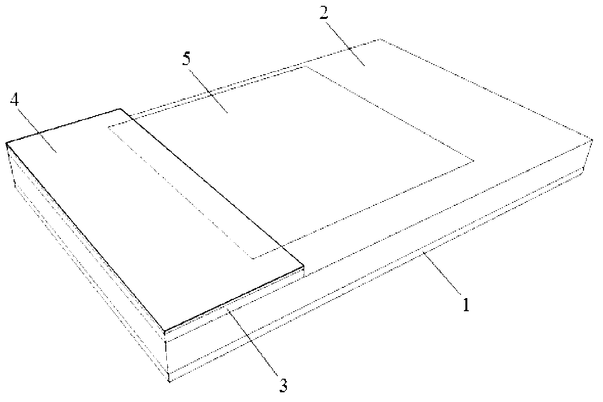
[0038] like figure 1Shown, the structure of p-type graphene film / n-type Ge Schottky junction near-infrared photodetector in the present embodiment is: take n-type Ge substrate 2 as the base region of near-infrared photodetector, in n The lower surface of the -type Ge substrate 2 is provided with an n-type Ge substrate electrode 1; the upper surface of the n-type Ge substrate 2 is covered with an insulating layer 3, and the area of ​​the insulating layer 3 is 1 / 5 to 1 / 5 of the area of ​​the n-type Ge substrate 2. 2 / 3, the boundary of the insulating layer 3 does not exceed the boundary of the n-type Ge substrate 2; the graphene contact electrode 4 is covered on the insulating layer 3, and the boundary of the graphene contact electrode 4 does not exceed the boundary of the insulating layer 3; A p-type graphene film 5 is laid on the contact electrode 4, a part of the p-type graphene film 5 is in contact with the graphene contact electrode 4, and the remaining part is in contact wi...

Embodiment 2

[0059] In the present embodiment, the structure of p-type graphene film / n-type Ge Schottky junction near-infrared photodetector is: with n-type Ge substrate 2 as the base region of near-infrared photodetector, in n-type Ge An n-type Ge substrate electrode 1 is provided on the lower surface of the substrate 2; an insulating layer 3 is covered on the upper surface of the n-type Ge substrate 2, and the area of ​​the insulating layer 3 is 1 / 5 to 2 / 3 of the area of ​​the n-type Ge substrate 2 , the boundary of the insulating layer 3 does not exceed the boundary of the n-type Ge substrate 2; the graphene contact electrode 4 is covered on the insulating layer 3, and the boundary of the graphene contact electrode 4 does not exceed the boundary of the insulating layer 3; the graphene contact electrode 4 A p-type graphene film 5 is laid on it, a part of the p-type graphene film 5 is in contact with the graphene contact electrode 4, and the remaining part is in contact with the part of th...


PUM

PropertyMeasurementUnit
Thicknessaaaaaaaaaa
Thicknessaaaaaaaaaa
Thicknessaaaaaaaaaa

Abstract

The invention discloses a p-type graphene film/n-type Ge schottky junction near-infrared photoelectric detector and a preparation method thereof. The p-type graphene film/n-type Ge schottky junction near-infrared photoelectric detector is characterized in that an n-type Ge substrate is used as a base region of a near-infrared photoelectric detector, and an n-type Ge substrate electrode is arranged on the lower surface of the n-type Ge substrate; the upper surface of the n-type Ge substrate is covered with an insulating layer, and the insulating layer does not go beyond the border of the n-type Ge substrate; the insulating layer is covered with a graphene contact electrode, and the graphene contact electrode does not go beyond the border of the insulating layer; and a p-type graphene film is laid on the graphene contact electrode, wherein a part of the p-type graphene film forms ohmic contact with the graphene contact electrode, the rest of the p-type graphene film forms schottky contact with the part, not covered with the insulating layer, of the upper surface of the n-type Ge substrate, and the p-type graphene film does not go beyond the border of the n-type Ge substrate electrode. The near-infrared photoelectric detector disclosed by the invention has the beneficial effects of large switch ratio, fast response speed and low dark current noise.

Description

technical field [0001] The invention belongs to the technical field of infrared photodetectors, and in particular relates to a p-type graphene film / n-type Ge Schottky junction near-infrared photodetector and a preparation method. Background technique [0002] Photodetectors can convert received optical signals into corresponding electrical signals, which have important military and market value. Among them, infrared detectors are widely used in military, national defense, fire protection, factory machine inspection, medical equipment and other fields. [0003] In 1800, F.W. Herschel discovered the presence of infrared radiation in the solar spectrum using a mercury thermometer, the original heat-sensitive infrared detector. With the development of infrared experiments and theory, new devices are constantly emerging. In 1873, W. Smith of England discovered the photoconductive effect of selenium, but this effect has been in the stage of exploration and research for a long ti...

Claims


Application Information

Patent Timeline
IPC IPC(8): H01L31/108H01L31/18
CPCY02P70/50
Inventor 罗林保曾龙辉谢超于永强梁凤霞
Owner HEFEI UNIV OF TECH
Why Eureka
Try Eureka