Patterned substrate and manufacturing method thereof
A technology for patterning substrates and manufacturing methods, applied in electrical components, circuits, semiconductor devices, etc., can solve problems such as reducing the light extraction efficiency of chips, and achieve the effects of improving light extraction efficiency and reducing losses
- Summary
- Abstract
- Description
- Claims
- Application Information
AI Technical Summary
Problems solved by technology
Method used
Image

Examples
Embodiment 1
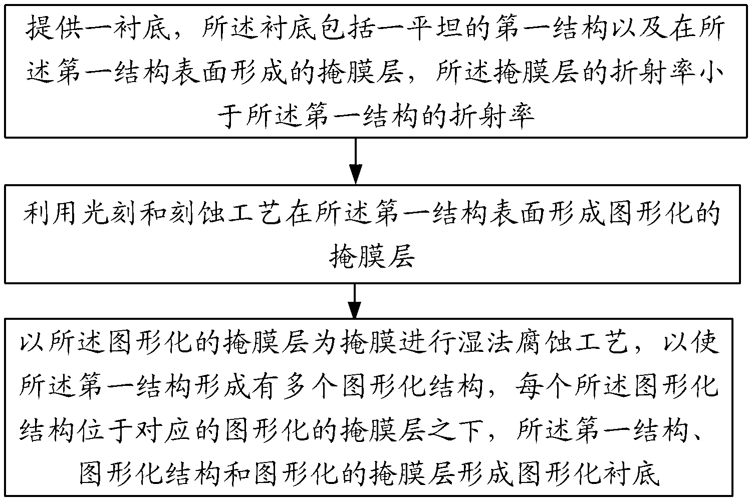
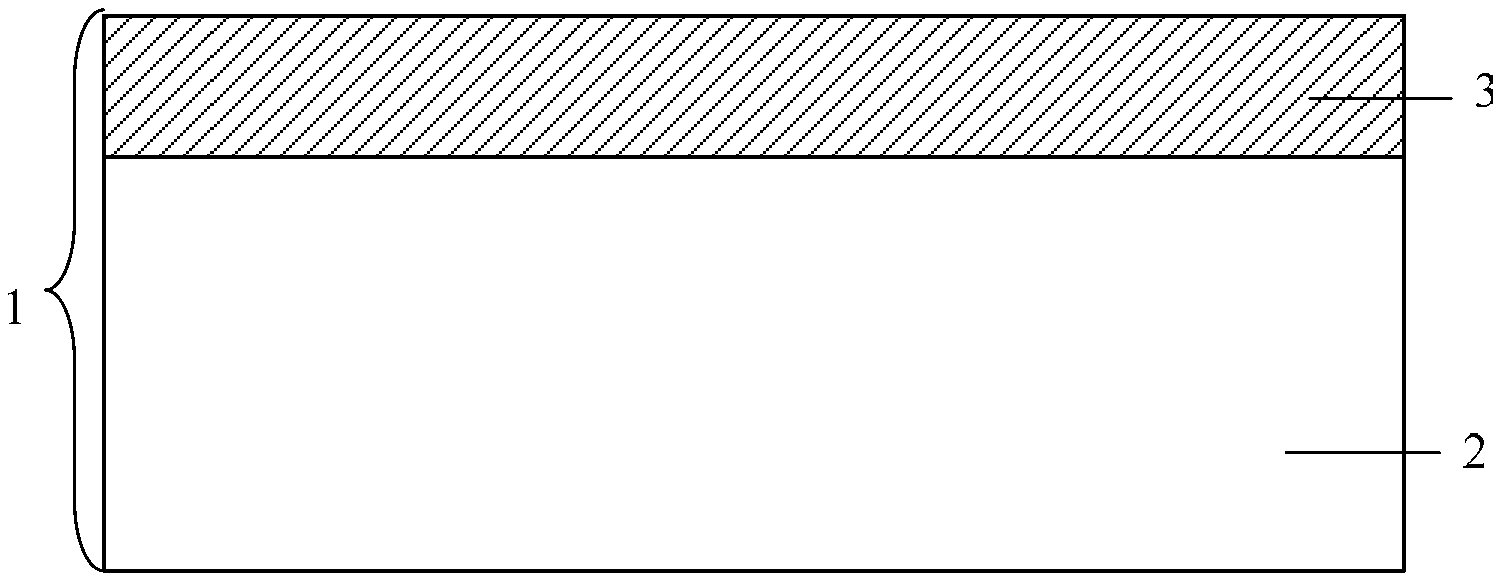
[0033] A substrate 1 is provided, the substrate 1 includes a flat first structure 2 and a mask layer 3 formed on the first structure 2, and the refractive index of the mask layer 3 is smaller than that of the first The refractive index of the structure 2, the material used in the first structure 2 is sapphire, the mask layer 3 is formed by depositing 70nm-90nm (nanometer) silicon dioxide by chemical vapor deposition process, preferably, the chemical The vapor deposition process can use plasma enhanced chemical vapor deposition (PECVD), such as Figure 2a shown;
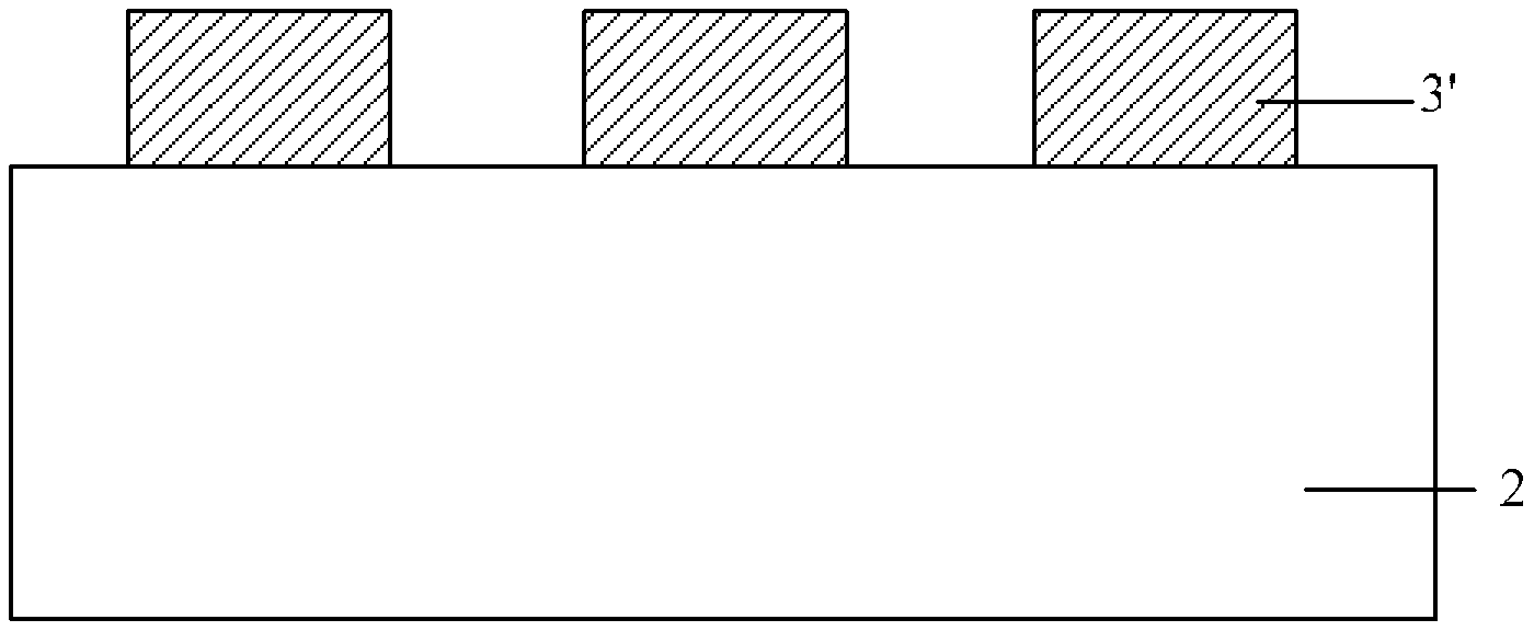
[0034] Removing part of the mask layer 3 by photolithography and buffered hydrofluoric acid (BOE) process, exposing the first structure 2, forming a patterned mask layer 3' on the surface of the first structure 2, get as Figure 2b the graph shown;
[0035] The parameters of a wet etching process are: temperature = 270°C, the mixed acid solution is phosphoric acid: sulfuric acid = 1:3 (volume ratio), the first stru...
Embodiment 2
[0037] A substrate 1 is provided, the substrate 1 includes a flat first structure 2 and a mask layer 3 formed on the first structure 2, and the refractive index of the mask layer 3 is smaller than that of the first The refractive index of the structure 2, the material used in the first structure 2 is sapphire, and the mask layer 3 is formed by depositing 100nm silicon nitride by a chemical vapor deposition process. Preferably, the chemical vapor deposition process can adopt Plasma Enhanced Chemical Vapor Deposition (PECVD), such as Figure 2a shown;
[0038] A part of the mask layer 3 is removed by photolithography and dry etching process to expose the first structure 2, and a patterned mask layer 3' is formed on the surface of the first structure 2 to obtain the following: Figure 2b the graph shown;
[0039] Using the wet etching process in Embodiment 1, the first structure 2 and the patterned mask layer 3' on it are soaked in the mixed acid solution for a certain period o...
PUM
| Property | Measurement | Unit |
|---|---|---|
| Thickness | aaaaa | aaaaa |
Abstract
Description
Claims
Application Information
 - Generate Ideas
- Intellectual Property
- Life Sciences
- Materials
- Tech Scout
- Unparalleled Data Quality
- Higher Quality Content
- 60% Fewer Hallucinations
Browse by: Latest US Patents, China's latest patents, Technical Efficacy Thesaurus, Application Domain, Technology Topic, Popular Technical Reports.
© 2025 PatSnap. All rights reserved.Legal|Privacy policy|Modern Slavery Act Transparency Statement|Sitemap|About US| Contact US: help@patsnap.com