MOS super barrier rectifier device and manufacturing method thereof

A rectifier device and super-barrier technology, which is applied in the field of power semiconductor devices, can solve the problems of device reliability reduction, semiconductor surface damage, high injection energy, etc., and achieve the goals of reducing reverse leakage current, improving stability, and reducing turn-on voltage Effect

Inactive Publication Date: 2013-09-25
ZHANGJIAGANG CASS SEMICON
View PDF6 Cites 9 Cited by
  • Summary
  • Abstract
  • Description
  • Claims
  • Application Information

AI Technical Summary

Problems solved by technology

In addition, the second conductivity type implantation area of ​​the existing patent ZL01143693.X only adopts the implantation method, and does not include the process of high temperature treatment. If such implantation is to achieve better results, higher implantation energy is required, and high-energy implantation Implantation damages the semiconductor surface seriously, and the reliability of the device is reduced

Method used


Image

  • MOS super barrier rectifier device and manufacturing method thereof
  • MOS super barrier rectifier device and manufacturing method thereof
  • MOS super barrier rectifier device and manufacturing method thereof

Examples


Embodiment Construction

[0042] The present invention will be further described in detail below through specific embodiments.

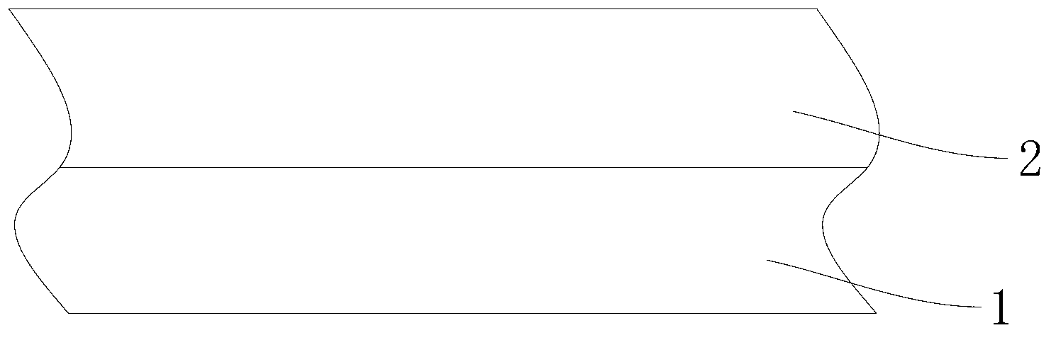
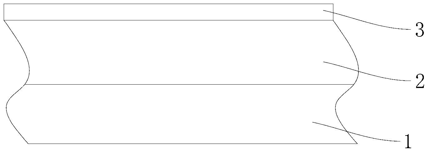
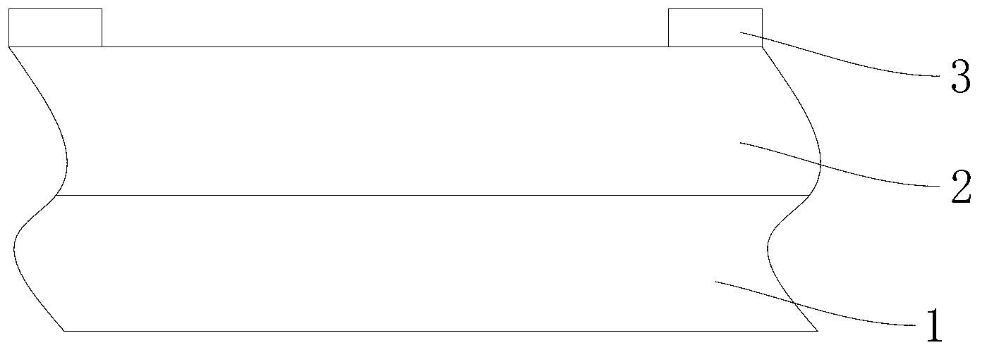
[0043] A MOS super-barrier rectifier device, such as Figure 12 As shown, the cross section of the rectifier device includes a semiconductor substrate, the lower part of the semiconductor substrate is a heavily doped first conductivity type substrate 1, the upper part of the semiconductor substrate is a lightly doped first conductivity type drift region 2, the The impurities of the first conductivity type may be N-type impurities, and correspondingly, the impurities of the second conductivity type mentioned below are P-type impurities, and vice versa. In this embodiment, the first conductivity type impurities are N-type impurities, and the second conductivity type impurities are P-type impurities. The upper surface of the semiconductor substrate is defined as the first surface, the lower surface of the semiconductor substrate is defined as the second surface, and the edge of...


PUM


Abstract

The invention discloses an MOS super barrier rectifier device which is provided with a groove, a second conduction type injection region wraps the groove, the structure can replace a protecting ring structure, a primary photomask is removed compared with the prior art, the depth of the second conduction type injection region is guaranteed, and good pressure proof functions are performed. In addition, the invention further discloses a manufacturing method. According to the method, after the groove is formed, the second conduction type injection region is injected and formed by carrying out heat treatment on activator impurities, the photomask needed when a protecting ring is formed and the processes of long-time trap pushing are removed, cost is saved, the damage, caused by injection by using macro-energy, to the surfaces of devices is avoided, transverse diffusion distance of micro-energy injection region is small, and the control over the length of a channel region and the distance between adjacent second conduction type injection regions is better.

Description

technical field [0001] The invention relates to a power semiconductor device, in particular to a MOS super-barrier rectifier device and a manufacturing method of the device. Background technique [0002] Existing power semiconductor rectifiers are divided into two types, one is a Schottky barrier rectifier, and the other is an integrated MOS channel super-barrier rectifier. [0003] The Schottky rectifier is a rectifier device made by contacting precious metals (such as gold, silver, platinum, titanium, nickel, molybdenum, etc.) with a semiconductor to form a Schottky barrier. Schottky barrier rectifiers have been gradually replaced by integrated MOS channel super-barrier rectifiers due to their high forward voltage drop, low reverse withstand voltage level, large reverse leakage current, and heavy metal pollution caused by the process. . [0004] Chinese patent ZL01143693.X discloses a "method of manufacturing semiconductor rectifier and obtained device", this patent give...

Claims


Application Information

Patent Timeline
Patent Type & Authority Applications(China)
IPC IPC(8): H01L29/78H01L29/06H01L21/336
Inventor 殷允超丁磊
Owner ZHANGJIAGANG CASS SEMICON
Why Eureka
Try Eureka