
Light emitting diode packaging structure and manufacturing method thereof

A technology of light-emitting diodes and packaging structures, applied in electrical components, electric solid devices, circuits, etc., can solve problems such as prolonging the life of unfavorable LED light sources, poor heat dissipation of LED light sources, and unfavorable heat dissipation of LED light sources, and achieves improved heat dissipation effect and good insulation. good heat dissipation effect

Inactive Publication Date: 2013-09-25
ELEC TECH OPTOELECTRONICS TECHWUHUCO
View PDF14 Cites 6 Cited by
  • Summary
  • Abstract
  • Description
  • Claims
  • Application Information

AI Technical Summary

Problems solved by technology

[0004] However, due to the low thermal conductivity of plexiglass or transparent inorganic glass, it is not conducive to heat dissipation of the LED light source, so the LED light source according to the above structure has poor heat dissipation, which is not conducive to prolonging the life of the LED light source

Method used


Image

  • Light emitting diode packaging structure and manufacturing method thereof
  • Light emitting diode packaging structure and manufacturing method thereof
  • Light emitting diode packaging structure and manufacturing method thereof

Examples


Embodiment Construction

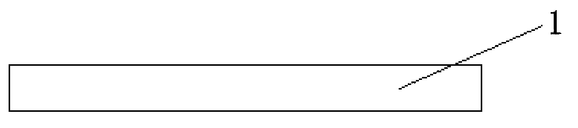
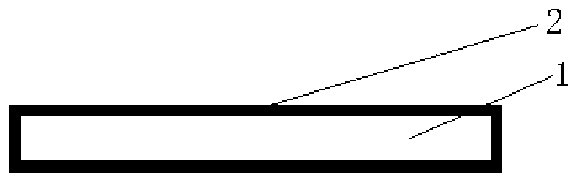
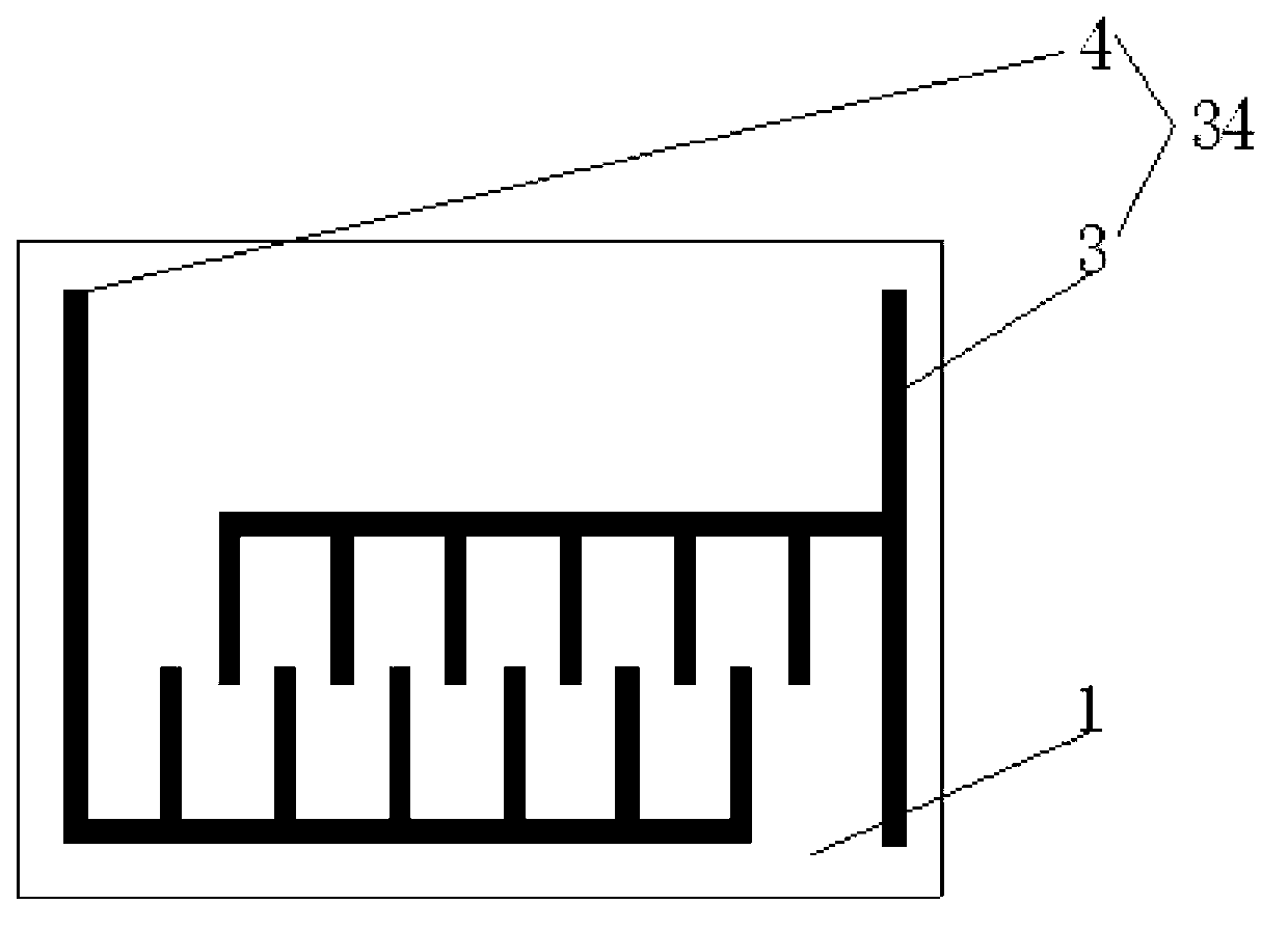
[0036] Such as Figure 1 to Figure 6 As shown, a light-emitting diode packaging structure provided by the present invention includes a transparent substrate 1, an LED chip 5 and a wire support 34, the wire support 34 is installed on the transparent substrate 1, the LED chip 5 is fixed on the transparent substrate, and the LED chip The electrodes of 5 are connected to the lead frame 34; the transparent substrate 1 is transparent glass or transparent sapphire substrate or transparent ceramic or organic transparent plastic.

[0037] Wherein, the light transmittance of the transparent substrate 1 is greater than 90%.

[0038] The single side, double side or three-dimensional surface of the transparent substrate 1 is evenly coated with a transparent high thermal conductivity film 2, and the required parameters of the transparent high thermal conductivity film 2 are: light transmittance greater than 90%, thermal conductivity greater than or equal to 400w / m·k; transparent The thickn...


PUM

PropertyMeasurementUnit
Thermal conductivityaaaaaaaaaa

Abstract

The invention relates to a light emitting diode packaging structure and a manufacturing method of the light emitting diode packaging structure. The light emitting diode packaging structure comprises a transparent substrate, an LED chip and a wire support which is installed on the transparent substrate. The LED chip is fixed on the transparent substrate. The electrode of the LED chip is connected with the wire support. The transparent substrate is made of transparent glass or a transparent sapphire substrate or transparent ceramic or organic transparent plastic. The transparent glass or the transparent sapphire substrate which is low in heat conducting coefficient is used as the transparent substrate, so that the heat radiating effect is good, the service life of the LED chip is beneficially prolonged, and then the service life of the light emitting diode packaging structure is beneficially prolonged.

Description

【Technical field】 [0001] The invention relates to the technical field of LEDs, in particular to a light emitting diode packaging structure and a manufacturing method thereof. 【Background technique】 [0002] Energy shortage is a hot topic in the world today. In the lighting industry, LED light source is the first choice to replace traditional lighting with high energy consumption and short life due to its advantages of high efficiency, energy saving, environmental protection, and long life. The chips of existing LED light sources are all packaged on non-transparent substrates, and the most commonly used non-transparent substrates are aluminum substrates. The defect of existing products is that the chip is packaged on a non-transparent substrate, part of the light is blocked by the non-transparent substrate, the maximum light emission angle is only 180 degrees, the utilization rate of light is low, the structure is single, and the production cost of the aluminum substrate stru...

Claims


Application Information

Patent Timeline
IPC IPC(8): H01L33/48H01L33/00
CPCH01L25/0753H01L33/62H01L2924/0002H01L2933/0033H01L2924/00
Inventor 王冬雷丁欣
Owner ELEC TECH OPTOELECTRONICS TECHWUHUCO
Features
  • Generate Ideas
  • Intellectual Property
  • Life Sciences
  • Materials
  • Tech Scout
  • Unparalleled Data Quality
  • Higher Quality Content
  • 60% Fewer Hallucinations
Learn More