Optical switching system based on arrayed waveguide grating

An arrayed waveguide grating and optical switching technology, which is applied in the field of optical network communication, can solve the problems of slow switching time and small number of ports, and achieve the effects of fast switching speed, compact structure, and single-chip integration

Active Publication Date: 2013-10-02
HUAZHONG UNIV OF SCI & TECH
View PDF2 Cites 9 Cited by
  • Summary
  • Abstract
  • Description
  • Claims
  • Application Information

AI Technical Summary

Problems solved by technology

[0003] One of the important technologies currently used to construct optical switching systems is the optical MEMS method, which has a large number of ports, but the biggest disadvantage is that the switching time is slow, only on the order of milliseconds; in addition, based on semiconductor optical amplifiers (SOA) The optical switch technology of piezoelectric ceramics (PLZT) can achieve nanosecond switching speed, but the number of ports is limited to a small scale, currently only 16×16 and 4×4
Considering that the requirements of the optical switching system in the existing optical network nodes are getting higher and higher, it must have the characteristics of multi-port, fast response time, and large capacity, so the above-mentioned optical switching system can no longer meet the current actual needs

Method used


Image

  • Optical switching system based on arrayed waveguide grating
  • Optical switching system based on arrayed waveguide grating
  • Optical switching system based on arrayed waveguide grating

Examples


Embodiment 1

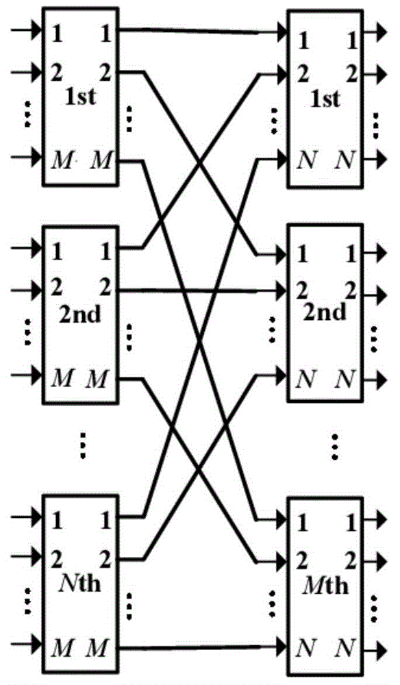
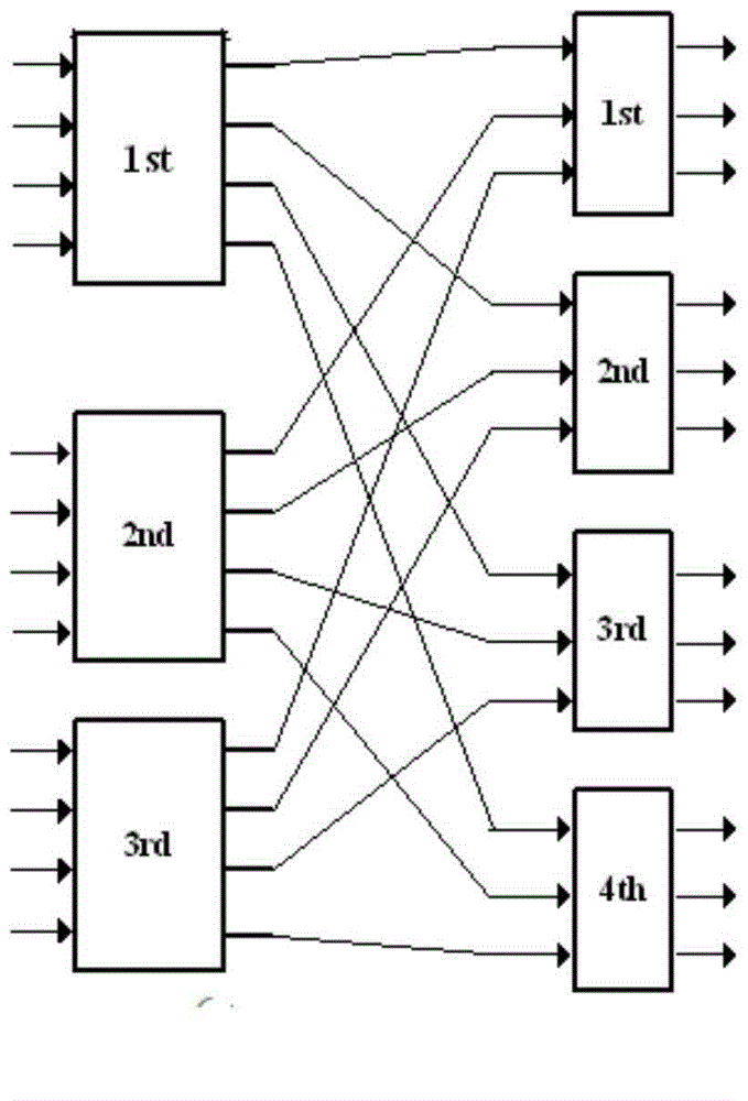
[0026] The following will refer to image 3 An example is used to illustrate the optical switching system constructed according to a preferred embodiment of the present invention. Such as image 3 As shown in , by setting M to 4 and N to 3, a large-scale optical switching system can be formed. Specifically, the first group of arrayed waveguide gratings in the front is composed of three 4×4 periodic arrayed waveguide gratings, and the second group of arrayed waveguide gratings in the rear is composed of four 3×3 periodic arrayed waveguide gratings. Furthermore, a 12×12 wavelength routing optical switching system is formed, and they can be directly connected by optical fibers, for example.

[0027] A more specific description can be given by taking the switching process from the first input port of the first periodic arrayed waveguide grating to any output port of the above optical switching system as an example:

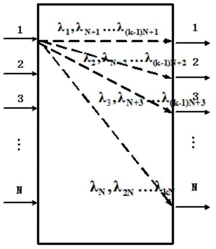
[0028] The wavelength of the loaded optical signal is set to ...

Embodiment 2

[0032] First, set M to 8 and N to 9. First, the first group and the second group of arrayed waveguide gratings are produced by monolithic integration, and the optical waveguide cross is used for linking, thus constructing a 72×72 wavelength routing Optical switching architecture.

[0033] In this embodiment, it is preferable to monolithically integrate nine 8×8 periodic arrayed waveguide gratings and eight 9×9 periodic arrayed waveguide gratings through silicon-on-insulator (SOI) technology, and integrate two groups of arrayed waveguide gratings The link between the two is realized by using the way of crossing the optical waveguide.


PUM


Abstract

The invention discloses an optical switching system based on arrayed waveguide gratings, which comprises an input unit, a switching unit and an output unit, wherein the switching unit comprises two groups of arrayed waveguide gratings, the preposed first group of arrayed waveguide gratings is composed of N M*M periodic arrayed waveguide gratings, the postposed second group of arrayed waveguide gratings is composed of M N*N periodic arrayed waveguide gratings; the output port of the first grating of the first group of arrayed waveguide gratings is sequentially linked with the first input ports of various gratings of the second group of arrayed waveguide gratings respectively; the output port of the second grating of the first group of arrayed waveguide gratings is sequentially linked with the second input ports of various gratings of the second group of arrayed waveguide gratings respectively; by parity of reasoning, the output port of the N-th grating of the first group of arrayed waveguide gratings is sequentially linked with the N-th input ports of various gratings of the second group of arrayed waveguide gratings respectively. Through the switching system, large scale port numbers are realized and response speed of nanosecond level is realized at the same time, and the system has the advantages of compact structure, easiness in operation and control, flexibility in use and the like, so that the system is particularly suitable for high-speed switching of an all-optical switching system.

Description

technical field [0001] The invention belongs to the technical field of optical network communication, and more specifically relates to an optical switching system based on an arrayed waveguide grating. Background technique [0002] At present, Internet data traffic and video communication services are showing explosive growth trends, which in turn has greatly increased the energy consumption of electrical switches and routers in traditional network electrical switching systems. The traditional electrical switching system is a process of optical-electrical-optical conversion. The light is converted into an electrical signal to pass through the switch and then converted back into light. This process not only limits the communication capacity, but also causes time delay and energy consumption. In order to solve this problem, the optical switch structure in the all-optical switching system has been gradually applied to the communication network due to its advantages of large cap...

Claims


Application Information

Patent Timeline
Patent Type & Authority Applications(China)
IPC IPC(8): G02B6/35G02B6/124
Inventor 张敏明戴竞刘德明
Owner HUAZHONG UNIV OF SCI & TECH
Why Eureka
Try Eureka