
Protection ring for preventing short circuit of test structure, and manufacturing method and package testing method thereof

A technology for testing structures and manufacturing methods, applied in semiconductor/solid-state device testing/measurement, semiconductor/solid-state device manufacturing, circuits, etc., can solve problems such as easy hitting of metal wire balls, operation errors, short-circuiting of test structures, etc. The effect of preventing moisture from entering the test structure

Active Publication Date: 2013-10-02
SHANGHAI HUALI MICROELECTRONICS CORP
View PDF5 Cites 4 Cited by
  • Summary
  • Abstract
  • Description
  • Claims
  • Application Information

AI Technical Summary

Problems solved by technology

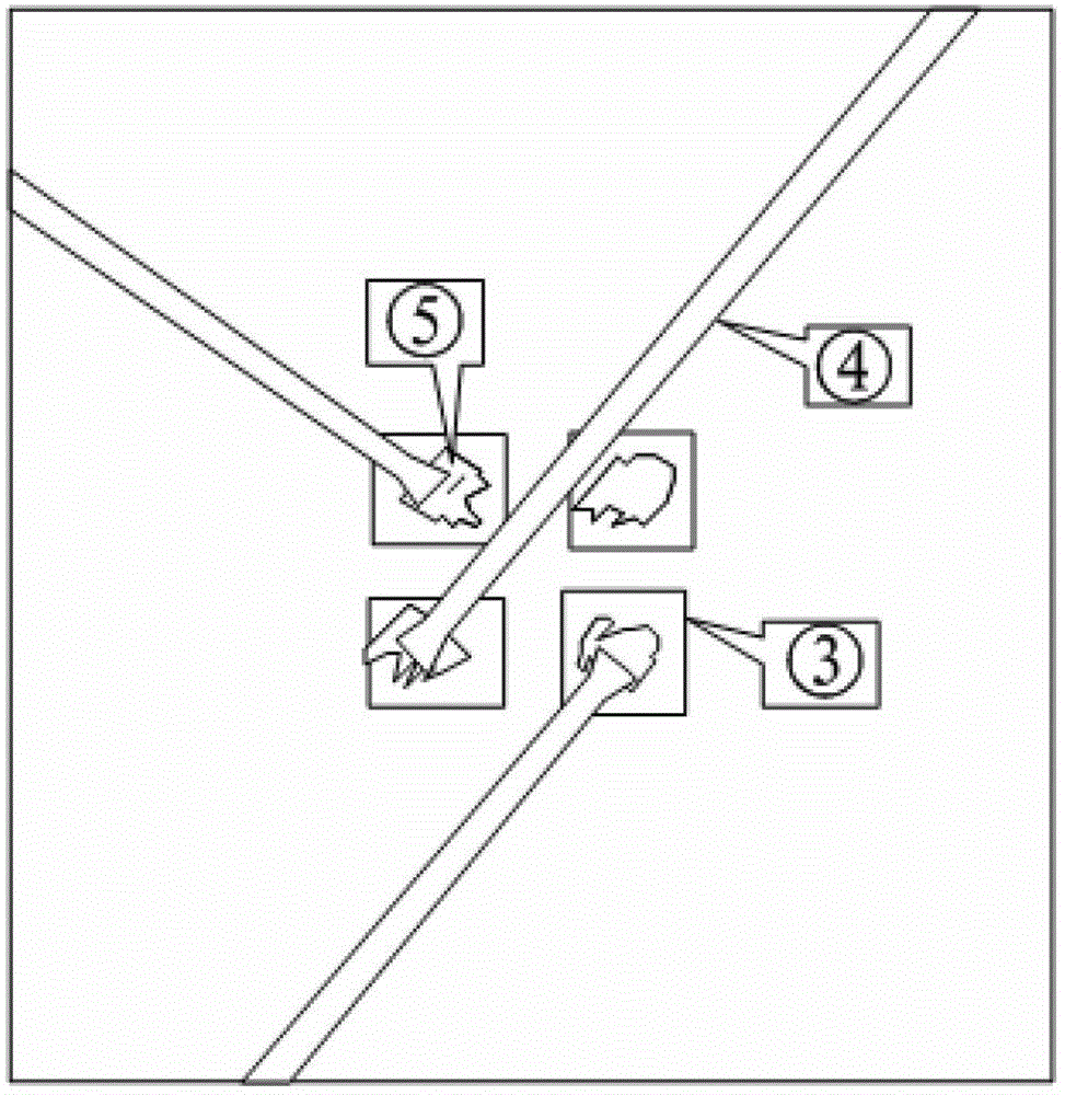
[0004] When the metal wire is connected to the ceramic base pin on the metal wire ball on the metal pad, the distance between the metal protection ring and the metal pad is limited due to the size of the metal pad being too small relative to the metal wire ball or the wiring error. , and the upper dielectric layer formed on the uppermost interconnection layer of the metal protection ring is one layer, and it is easy for the metal connection ball to hit the metal pad. Layer ⑦, so it will cause the hidden danger of short circuit in the test structure, such as Figure 5 as shown, Image 6 It is a partially enlarged top view, ⑧ is the connection line between the test structure and the metal pad
[0005] For this reason, it is urgent to provide a new protective ring to avoid the contact between the metal connecting ball and the protective ring due to the metal pad being too small or operating errors or the thickness of the upper dielectric layer making the metal connecting ball part reach the metal pad. The short-circuit problem caused by the test structure

Method used


Image

  • Protection ring for preventing short circuit of test structure, and manufacturing method and package testing method thereof
  • Protection ring for preventing short circuit of test structure, and manufacturing method and package testing method thereof
  • Protection ring for preventing short circuit of test structure, and manufacturing method and package testing method thereof

Examples


Embodiment 1

[0042] by Figure 7 The flow chart shown in the example, combined with Figure 8 , and describe in detail the manufacturing method of a guard ring for preventing short circuit of the test structure provided by the present invention.

[0043] In step 1, a low-K dielectric layer 100 is formed, grooves are opened in the low-K dielectric layer, and metal is filled to form an interconnection layer with a metal belt-shaped surrounding structure. The interconnection layer formed for the first time is used as the bottom interconnection layer 201 .

[0044]In step 2, step 1 is repeated, and the interconnection layer as described in step 1 is formed on the underlying interconnection layer, and the interconnection layer formed for the second time is used as the bottom metal via 202; and step 1 is repeated, and the bottom metal via The interconnection layer as described in step 1 is formed on the upper layer, and the interconnection layer formed for the third time is used as the sub-bott...

Embodiment 2

[0050] by Figure 9 The flow chart shown in the example, combined with Figure 10 , a package testing method for preventing a short circuit of a test structure provided by the present invention is described in detail.

[0051] In step 10, the guard ring 500 for preventing short circuit of the test structure is formed on the wafer.

[0052] In step 20, the wafer is subjected to water dicing to obtain the protection ring for preventing short circuit of the test structure.

[0053] In step 30, a ceramic base is provided, the ceramic base has a placement area and ceramic base pins, the protective ring for preventing short circuit of the test structure is placed on the placement area, and the prevention ring of the test structure is placed on the placement area. A shorted guard ring with a guarded test structure. In this embodiment, in fact, when the ceramic base can put down the protective ring for preventing the short circuit of the test structure, the larger the cut of the pr...


PUM


Abstract

The invention provides a protection ring for preventing short circuit of a test structure, and a manufacturing method and a package testing method thereof. The protection ring comprises a separating structure, three upper medium layers and a plurality of metal pads, wherein the separating structure comprises a plurality of the same interconnection layers which are sequentially connected layer by layer from the bottom up; a metal-strip-like enclosing structure is arranged in each interconnection layer; the metal-strip-like enclosing structure is formed by grooving a low-K medium layer and filling grooves with metal; the three upper medium layers are formed in the separating structure; windows are formed in the three upper medium layers; the metal pads are formed in the low-K medium layers enclosed by the metal-strip-like enclosing structures; each window corresponds to a metal pad, thus preventing the performance worsening problem of the test structure caused by water entering the test structure in the slice packaging process or other operating process, and avoiding the short circuit problem of the test structure caused by contact of a metal ball connecting ball and the protection ring because a part of the metal ball connecting ball is outside the metal pad due to too small metal pads or operating errors.

Description

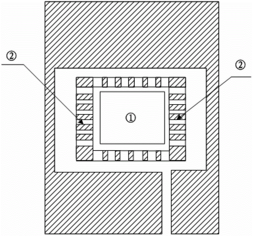
technical field [0001] The invention belongs to the technical field of semiconductor chip packaging, and in particular relates to a protection ring for preventing short circuit of a test structure, a manufacturing method thereof, and a packaging and testing method. Background technique [0002] When the test structure needs to be tested at the package level, the test structure will punch metal connection balls on the metal pads of the corresponding test structure, and then connect metal wires to the ceramic base pins on the metal connection balls, such as figure 1 As shown in the structure of the ceramic base, ① is the test structure placement area, ② is the pin of the ceramic base, figure 2 It is an enlarged view of the test structure after packaging, ③ is a metal pad, ④ is a metal wire, and ⑤ is a metal connection ball. Wafer dicing needs to be carried out in a water environment. Water will diffuse to all parts of the test structure through the dielectric layer (inorgani...

Claims


Application Information

Patent Timeline
Patent Type & Authority Applications(China)
IPC IPC(8): H01L21/66H01L21/762H01L23/528H01L23/58
Inventor 赵敏尹彬锋王炯
Owner SHANGHAI HUALI MICROELECTRONICS CORP
Learn More