Heavy-copper step circuit board and preparation method thereof

A circuit board and ladder technology, which is used in the manufacture of printed circuits, removal of conductive materials by chemical/electrolytic methods, and printed circuits. It can solve the problems of easy scratching, low production efficiency, and long plating time, and achieve high economic Benefit, low cost, and the effect of solving the line gap

Active Publication Date: 2013-10-02
KALEX MULTI LAYER CIRCUIT BOARD (ZHONGSHAN) CO LTD
View PDF5 Cites 24 Cited by
  • Summary
  • Abstract
  • Description
  • Claims
  • Application Information

AI Technical Summary

Problems solved by technology

The disadvantage of this patented technology is: the conductive layer formed by sinking copper is extremely thin (0.3-0.5um), and it is very easy to scratch during the mask operation, which will bring quality problems
At the same time, for the stepped circuit with a large height difference, the conductive layer is thin, and in order to obtain the required thickness, it takes a long time for electroplating, and the production efficiency is low

Method used


Image

  • Heavy-copper step circuit board and preparation method thereof
  • Heavy-copper step circuit board and preparation method thereof
  • Heavy-copper step circuit board and preparation method thereof

Examples


Embodiment 1

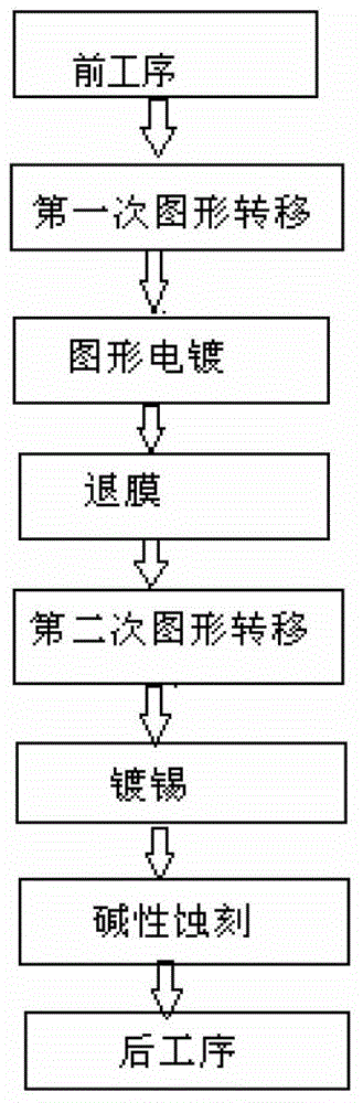
[0043] Embodiment 1 The preparation method of 3OZ thick copper stepped circuit board

[0044] see figure 1 , is the preparation process diagram of the thick copper stepped circuit board of the present invention. In this embodiment, the thin copper lines are 1OZ and the thick copper lines are 3OZ. Prepared by the following procedure:

[0045] 1. Pre-process

[0046] That is, the copper sinking electrical process is an existing conventional technology, and will not be repeated here.

[0047] 2. The first graphics transfer

[0048] Using a positive film with only thick copper lines, the process flow is grinding plate-roller film-exposure-development;

[0049]In the next process of graphic plating for thick copper stepped circuit boards, some lines will be thickened from thin copper to thick copper lines; there is a large difference between thick and thin lines, and the use of conventional 2mil dry film in the roll film process will cause quality problems with the film cl...

Embodiment 2

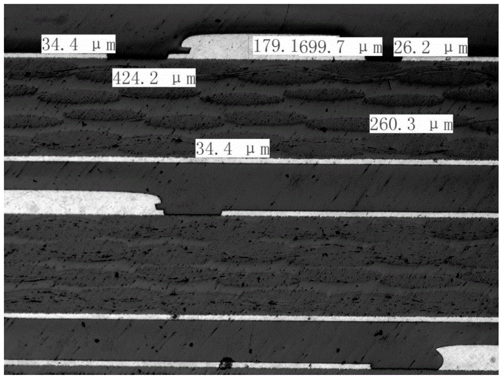
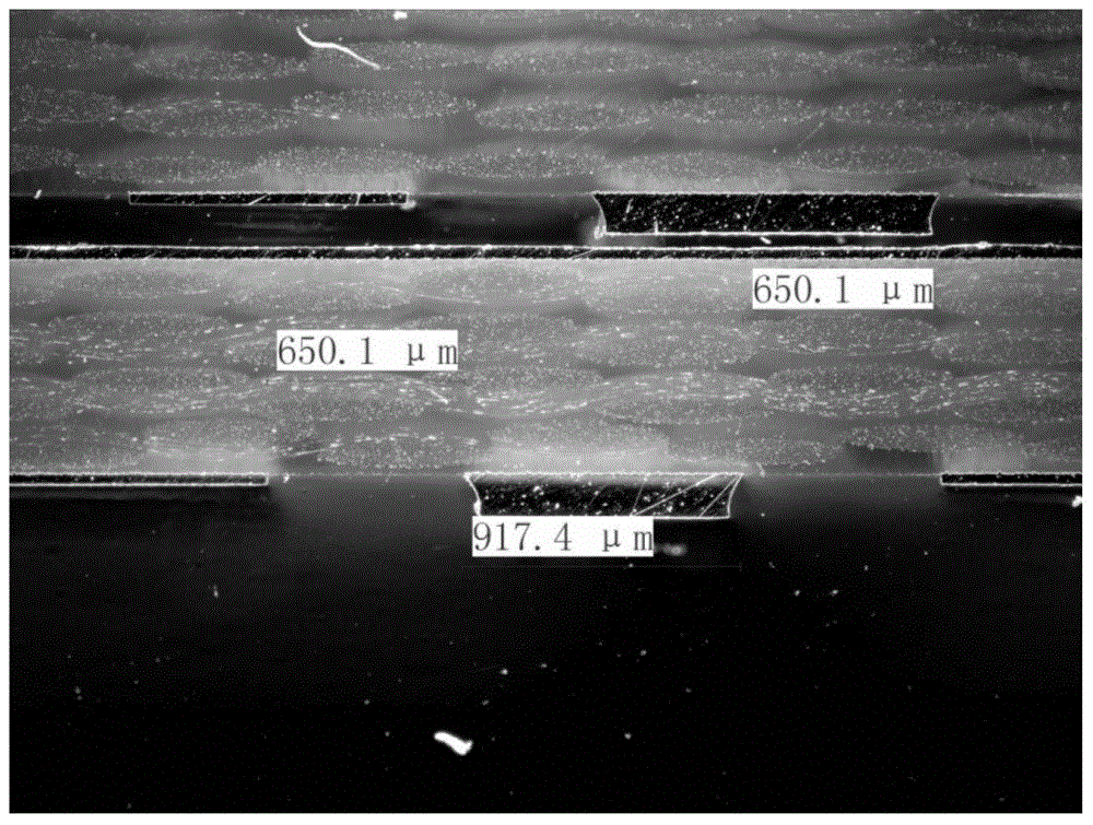
[0074] The thick copper step plate of the present embodiment is compared with the microsection of the step plate prepared by traditional technology, and the results are as follows: figure 1 and figure 2 As shown, the results show that: the stepped plate prepared by the traditional process has film clips, but the stepped plate prepared by the process of this embodiment has no film clips, therefore, the preparation method of the present invention meets the requirements. Embodiment 2 The preparation method of 3OZ thick copper stepped circuit board

[0075] The preparation method of the thick copper ladder circuit board of this embodiment is all identical with the step of embodiment 1 except that following steps are different from embodiment:

[0076] 2. The first graphics transfer

[0077] A layer of 2mil dry film is used in the rolling film process. After the plate is rolled normally, take the plate, tear off the protective film, put it into the rolling machine and roll the...

Embodiment 3

[0087] Embodiment 3 The preparation method of 6OZ ultra-thick copper stepped circuit board

[0088] In this embodiment, the thin copper lines are 1OZ and the thick copper lines are 6OZ.

[0089] The preparation method of the thick copper ladder circuit board of this embodiment is all identical with the step of embodiment 1 except that following steps are different from embodiment:

[0090] 2. The first graphics transfer

[0091] In this example, two layers of 2mil dry film are used in the roll film process. After the plate is normally rolled once, take the plate, tear off the protective film, put it into the roll machine and roll the film again; the roll plate parameters are: roll plate pressure 4kg / cm 2 , the temperature of the hot reel is 110°C, the speed of the reel is 2.0m / min, and the temperature of the plate is 55°C;

[0092] 3. Graphic plating

[0093] In this embodiment, the electroplating current density is 21ASF, and the electroplating time is 270min.

[00...


PUM


Abstract

The invention discloses a heavy-copper step circuit board and a preparation method thereof. The preparation method comprises the working procedures of primary pattern transfer, pattern electroplating, film removal, secondary pattern transfer, tinning and alkaline etching. The preparation method solves the quality problem of a clamping film and the quality problems such as circuit nicks and unclean etching due to the fact that an anti-corrosion layer cannot be closely bonded with a circuit by a dry film technology by utilizing the production capacity of the available equipment and optimizing roll film, board grinding and etching processes; the whole preparation process is compatible with the traditional circuit board technology; and the quality and the cost can be compatible effectively.

Description

technical field [0001] The invention belongs to the field of printed circuit board (PCB), and more specifically, the invention relates to a thick copper stepped circuit board and a preparation method thereof. Background technique [0002] Thick copper circuit boards are used as automotive electronic components, especially in high-power and high-voltage parts such as engine power supply parts and automotive central electrical power supply parts. The circuit boards are required to have high reliability characteristics such as heat aging resistance and high and low temperature cycle resistance. [0003] In addition to ensuring the reliability of heat dissipation of the product, it is also necessary to ensure the performance of the product and control the cost of the product. There are different line thickness requirements in different parts of the circuit board. In the production of circuit boards, thick copper stepped circuit boards appeared; thick Copper stepped circuit board...

Claims


Application Information

Patent Timeline
Patent Type & Authority Applications(China)
IPC IPC(8): H05K3/00H05K3/06H05K1/00
Inventor 霍嘉昌任利春
Owner KALEX MULTI LAYER CIRCUIT BOARD (ZHONGSHAN) CO LTD
Why Eureka
Try Eureka