Silicon substrate radial homojunction heterojunction solar battery and manufacturing method thereof

A solar cell and heterojunction technology, which is applied in circuits, photovoltaic power generation, electrical components, etc., can solve the problems of affecting the interface state density, reducing the interface state density, and interface state density sensitivity, so as to improve performance and reduce costs Effect

Active Publication Date: 2013-10-09
SHANGHAI JIAO TONG UNIV
View PDF7 Cites 11 Cited by
  • Summary
  • Abstract
  • Description
  • Claims
  • Application Information

AI Technical Summary

Problems solved by technology

[0005] However, the introduction of the intrinsic amorphous silicon film reduces the interface state density and increases the series resistance of the battery (due to the high resistivity characteristics of the intrinsic amorphous silicon film)
In addition, the linear array surface structure of radial PN junction cells ...

Method used


Image

  • Silicon substrate radial homojunction heterojunction solar battery and manufacturing method thereof
  • Silicon substrate radial homojunction heterojunction solar battery and manufacturing method thereof
  • Silicon substrate radial homojunction heterojunction solar battery and manufacturing method thereof

Examples


Embodiment 1

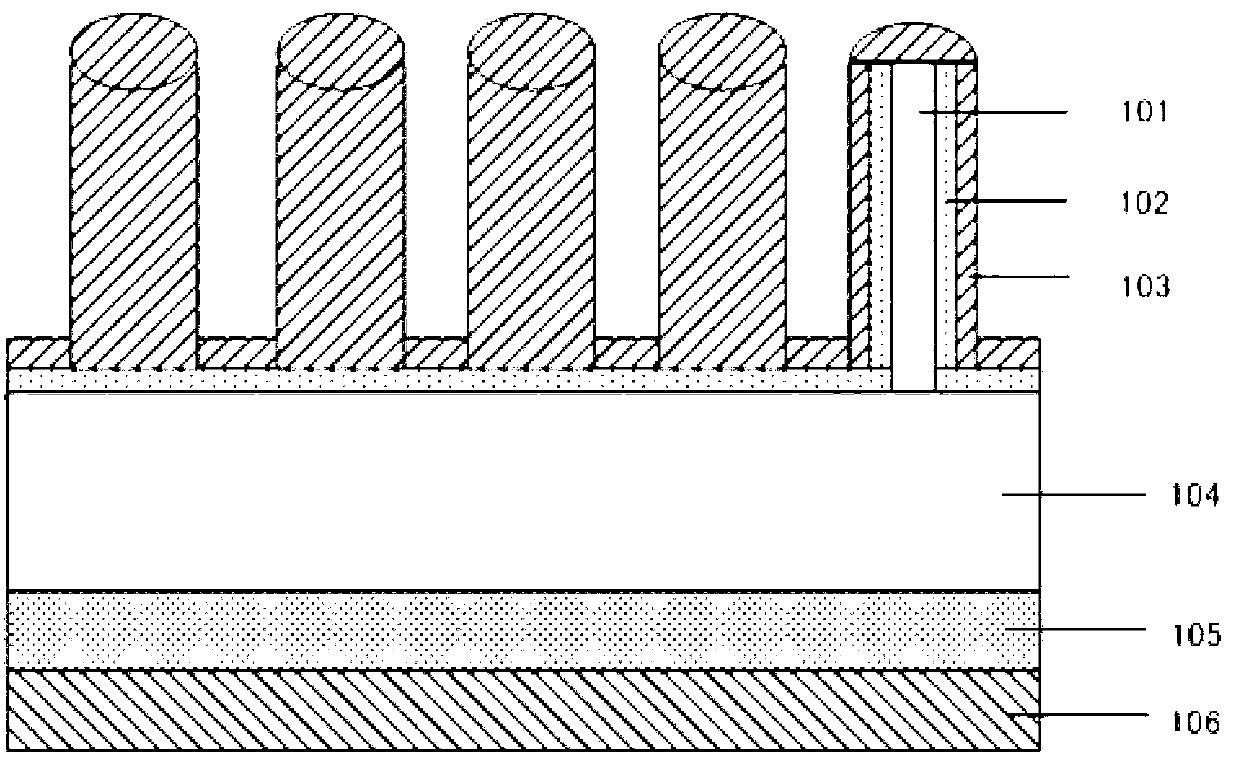
[0036] The battery structure includes, as figure 1 As shown, the silicon substrate 104 is P-type single crystal silicon (P-c-Si); the inner layer 101 of each silicon line is P-type single crystal silicon (P-c-Si), and the middle layer 102 is N-type doped single crystal silicon (N-c-Si), the shell layer 103 is an N+ type amorphous silicon film (N + -a-Si); the front of the silicon substrate 104 forms a submicron or micron silicon line array; the back of the silicon substrate 104 is, from top to bottom, an intrinsic I-type amorphous silicon film 105 (I-a-Si) and a P+ type Amorphous silicon film 106 (P + -a-Si), constituting the HIT structure. The front side of the P-type crystalline silicon wafer is a submicron or micron silicon line array, PN homogeneous NN+ heterojunction structure, the homojunction is the radial homojunction of crystalline silicon, and the heterojunction is the radial heterojunction of crystalline silicon / amorphous silicon Mass junction; the back of the si...

Embodiment 2

[0045] The battery structure includes, as figure 1 As shown, the silicon substrate 104 is P-type single crystal silicon (P-c-Si); the inner layer 101 of each silicon line is P-type single crystal silicon (P-c-Si), and the middle layer 102 is N-type doped single crystal silicon (N-c-Si), the shell layer 103 is N + type amorphous silicon film (N + -a-Si); the front side of the silicon substrate 104 forms a submicron or micron silicon line array; the back side of the silicon substrate 104 is an intrinsic I-type amorphous silicon film 105 (I-a-Si) and P + type amorphous silicon film 106 (P + -a-Si), constituting the HIT structure. The front side of the P-type crystalline silicon wafer is a submicron or micron silicon line array, PN homogeneous NN+ heterojunction structure, the homojunction is the radial homojunction of crystalline silicon, and the heterojunction is the radial heterojunction of crystalline silicon / amorphous silicon Mass junction; the back of the silicon wafer i...

Embodiment 3

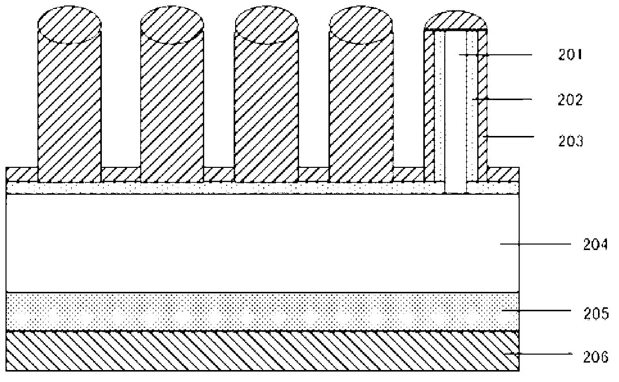
[0054] The battery structure includes, as figure 2 As shown, the silicon substrate 204 is P-type single crystal silicon (P-c-Si); the inner layer 201 of each silicon line is P-type single crystal silicon (P-c-Si), and the middle layer 202 is N-type doped single crystal silicon (N-c-Si), the shell layer 203 is N + type amorphous silicon film (N + -a-Si); the front side of the silicon substrate 204 forms a submicron or micron silicon line array; the back side of the silicon substrate 204 is P from top to bottom + type monocrystalline silicon 205 (P + -c-Si) and P ++ type amorphous silicon film 206 (P ++ -a-Si), forming PP + Homogeneous concentration junction and P + P ++ Heterogeneous concentration junction. The front side of the P-type crystalline silicon wafer is a submicron or micron silicon line array, PN homogeneous NN + Heterojunction structure, the homojunction is the radial homojunction of crystalline silicon, the heterojunction is the radial heterojunction of ...


PUM

PropertyMeasurementUnit
Diameteraaaaaaaaaa
Heightaaaaaaaaaa
Doping concentrationaaaaaaaaaa

Abstract

The invention discloses a silicon substrate radial homojunction heterojunction solar battery and a manufacturing method of the silicon substrate radial homojunction heterojunction solar battery. The silicon substrate radial homojunction heterojunction solar battery comprises a silicon substrate and a silicon line array on the silicon substrate. Each silicon line in the silicon line array comprises an inner layer, a middle layer and an outer shell layer, a radial PN junction is formed between the inner layer and the middle layer of each silicon line, and a radial heterojunction is formed between the middle layer and the outer shell layer of each silicon line. The PN junctions are homojunctions, the homojunctions are crystalline silicon PN junctions, PP+ concentration junctions or NN+ concentration junctions, and the heterojunctions are crystalline silicon/noncrystalline silicon PP+ concentration junctions, P+P++ concentration junctions, N+N++ concentration junctions, NN+ concentration junctions, NI junctions or PI junctions. The advantages of a radial PN junction battery and the advantages of a homojunction heterojunction battery are combined by the silicon substrate radial homojunction heterojunction solar battery sufficiently, therefore, the high photoelectric conversion efficiency can be achieved on low-quality silicon materials, and meanwhile the performance stability of the silicon substrate radial homojunction heterojunction solar battery is improved.

Description

technical field [0001] The invention relates to the field of new energy, in particular to a radial homogeneous heterojunction solar cell based on a silicon substrate and a preparation method thereof. Background technique [0002] With the problems of environmental pollution and the depletion of traditional energy sources, solar cells, as an important development direction of new energy sources, have attracted more and more attention from all over the world. Improving efficiency and reducing cost are eternal topics in the development of solar cells. For silicon cells, the cost of silicon material is an important part of the cost of the cell. Therefore, using low-grade silicon wafers and reducing the thickness of silicon wafers can effectively reduce the cost of silicon solar cells. For example, the cost of metallurgical grade silicon is only 1.75-2.30$ / kg, far lower than the current solar grade silicon, but its purity cannot meet the requirements of conventional crystalline...

Claims


Application Information

Patent Timeline
IPC IPC(8): H01L31/18H01L31/078H01L31/0352
CPCY02E10/50Y02P70/50
Inventor 沈文忠钟思华韩旭根
Owner SHANGHAI JIAO TONG UNIV
Why Eureka
Try Eureka