Multi-stage single switch boost converter

A boost converter, single-switch technology, applied in instruments, converting DC power input to DC power output, adjusting electrical variables, etc., can solve the problems of high voltage stress of switching tubes, low input voltage utilization rate, and many inductive components. , to meet the requirements of reducing the capacity of the capacitor withstanding voltage, high utilization of power supply voltage, and simple control circuit.

Inactive Publication Date: 2013-10-09
CHONGQING UNIV
View PDF4 Cites 13 Cited by
  • Summary
  • Abstract
  • Description
  • Claims
  • Application Information

AI Technical Summary

Problems solved by technology

[0003] At present, in the field of new energy grid-connected power generation, the traditional Boost converter is widely used. However, in practical applications, its boosting capacity is limited, only 6 times the input voltage. If the output voltage is to be continuously increased, the To increase the duty cycle, this will cause the following problems: ①The voltage and current stress of the active switch tube and diode are large; ②The switching loss and diode reverse recovery loss are large, resulting in low conversion efficiency; ③The dv / dt is large, Lead to serious EMI; ④ Poor ability to resist input voltage disturbance and dynamic performance
Although the current device can achieve a better boost effect, the topology is complex, the design of the control circuit is difficult, and there are many inductive components, and the converter is bulky.
Although the existing n-level cascaded Boost converter can achieve high boosting capability, the voltage stress of the switching tube is relatively high, which is equal to the output voltage, which affects the working efficiency of the converter.
Someone proposed the Z-source converter topology, which uses a unique impedance network to couple the main circuit of the converter and the power supply together to obtain unique characteristics that cannot be obtained by traditional voltage source and current source converters, and provides a novel power converter. The transformation concept overcomes the deficiencies of the traditional voltage source and current source converters, but there are deficiencies in the aspects of insufficient boosting capacity, severe start-up shock, and low DC voltage utilization due to intermittent input current.
The method of cascaded quasi-Z source impedance network is used to increase the voltage gain, and the conversion efficiency is high, but the topology of the main circuit and the control circuit are more complicated. How to ensure the stable operation of the cascaded quasi-Z source impedance network is also relatively difficult, and the circuit There are many inductive components and the volume is large
The existing Cuk converter and Sepic converter use voltage bootstrap technology to realize boosting effect. Although the input current ripple and output voltage ripple are small and the control circuit is simple, the boosting capability is limited.
At present, it is also proposed to use coupled inductors to build high-boost converters for fuel cell power generation systems. The use of coupled inductors will cause excessive voltage stress on switching devices, resulting in large operating losses, low efficiency, and more active switching elements in the converter. ,high cost
Although some schemes recorded in the literature can achieve a good boost effect, the topology is relatively complex, the design of the control circuit is difficult, and the utilization rate of the input voltage is low, and the output voltage ripple is large.

Method used


Image

  • Multi-stage single switch boost converter
  • Multi-stage single switch boost converter
  • Multi-stage single switch boost converter

Examples


Embodiment 1 2

[0037] Embodiment 1 Two-stage single-switch boost converter

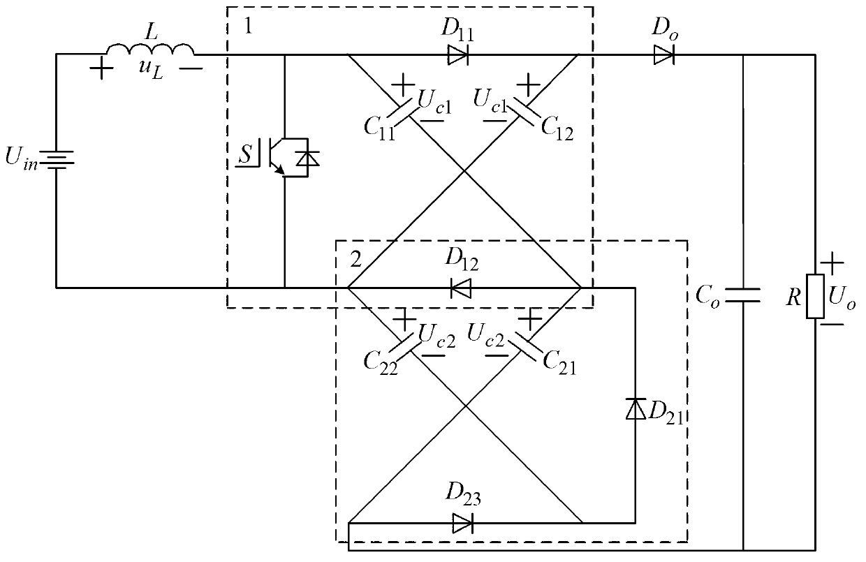
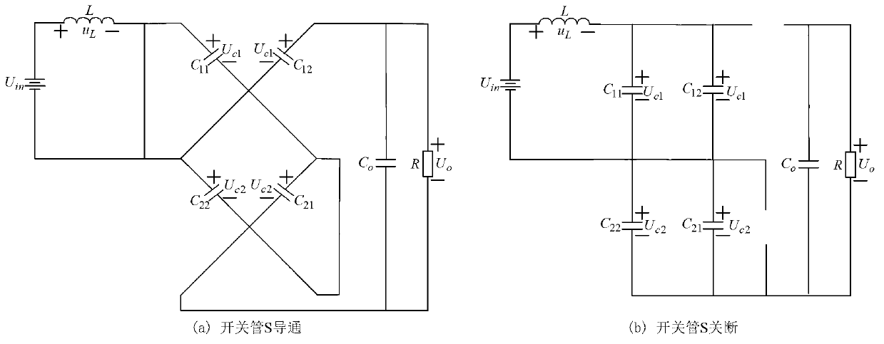
[0038] Add a Switch-Capacitor network to the pre-stage Boost network to form a secondary single-switch boost converter, such as figure 1 shown. Denote these two nets as net 1 and net 2, where net 1 and net 2 share diode D 12 . The equivalent circuit of the two-stage single-switch boost converter is shown as figure 2 shown.

[0039] When the active switch S is turned on, the diode D 11 、D 12 、D 23 Deadline, D 21 、D o conduction, the equivalent circuit of the secondary single-switch boost converter is as figure 2 (a) shown. At this point, the capacitor C in network 1 11 with C 12 and capacitor C in network 2 21 with C 22 respectively interleaved in series, while the capacitance C 11 with C 22 in parallel.

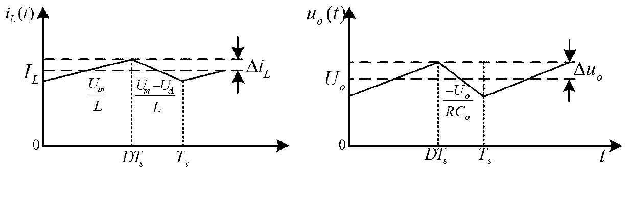
[0040] The voltage across the inductor L is:

[0041] u L =U in (1-1)

[0042] due to C 11 with C 22 In parallel, so the capacitor voltages in network 1 and network 2 are equal, that is:...

Embodiment 2 3

[0059] Embodiment 2 Three-stage single-switch boost converter

[0060] If a Switch-Capacitor network is added on the basis of Embodiment 1, a three-stage single-switch boost converter can be formed, such as Figure 4 shown, where net 1 and net 2 share diode D 12 , net 2 and net 3 share diode D 23 . Its equivalent circuit is as Figure 5 shown.

[0061] When the active switch S is turned on, the diode D 11 、D 12 、D 23 、D 34 Deadline, D 21 、D 31 、D o conduction, its equivalent circuit is as Figure 5 (a) shown. At this point, the capacitor C in network 1 11 with C 12 , the capacitor C in network 2 21 with C 22 and capacitor C in network 3 31 with C 32 respectively interleaved in series, while C 11 with C 22 、C 21 with C 32 respectively in parallel.

[0062] The voltage across the inductor L is:

[0063] u L =U in (2-1)

[0064] due to C 11 with C 22 、C 21 with C 32 They are connected in parallel respectively, so the capacitance voltages in these...

Embodiment 3

[0078] Embodiment 3 Multi-level single-switch boost converter

[0079] Based on the composition law and working principle of the two-stage single-switch boost converter and the three-stage single-switch boost converter, if (n-1) Switch-Capacitor networks are added to the previous Boost network, we can get A boost converter with n networks is referred to as an n-level single-switch boost converter, also known as a multi-level single-switch boost converter. Its circuit topology is as follows: Figure 7 shown.

[0080] Depending on the number of Switch-Capacitor networks interleaved in series, the converter structure will be different, but generally speaking, it can be divided into two topological structures, such as Figure 7 shown. Note that the number of interleaved networks is n, when n=2k (k is a positive integer), the topology is as follows Figure 7 As shown in (a), there are an even number of Switch-Capacitor networks interleaved in series; when n=2k+1 (k is a positive...


PUM


Abstract

The invention relates to the field of power electronics, in particular to a multi-stage single switch boost converter which is composed of a Boost circuit and a plurality of Switch-Capacitor networks. Voltages supplied by all the Switch-Capacitor networks are equal. Accumulation of the network voltages is achieved in an interleaving series connection mode, an output voltage is boosted, and the capacity of boosting is high. The converter is provided with only one active switch element, a control circuit is simple, and voltage stress of a switching tube is small and 1/ (1-D) times that of an input voltage. Capacitor voltages of all the Switch-Capacitor networks are equal and 1/ (1-D) times that of the input voltage, stress of the capacitor voltages is small, therefore, the size of the circuit is reduced, and integration is easy.

Description

technical field [0001] The invention relates to the field of power electronics, in particular to a multi-stage single-switch boost converter. Background technique [0002] In renewable energy grid-connected power generation, photovoltaic power generation and fuel cell power generation play an important role. However, the output voltages of solar panels and fuel cells are relatively low, which is not enough to achieve the purpose of grid-connected power generation. Therefore, a DC-DC boost converter with a larger boost ratio becomes extremely important. In addition, in order to be suitable for the engineering field, this type of boost converter should also have smaller volume, higher power density and higher efficiency. [0003] At present, in the field of new energy grid-connected power generation, the traditional Boost converter is widely used. However, in practical applications, its boosting capacity is limited, only 6 times the input voltage. If the output voltage is to ...

Claims


Application Information

Patent Timeline
Patent Type & Authority Applications(China)
IPC IPC(8): H02M3/155H02M1/14
Inventor 侯世英陈剑飞孙韬邹学伟张立帅陈复梁涛龚嫄
Owner CHONGQING UNIV
Why Eureka
Try Eureka