High reliability smd LED packaging structure
A packaging structure and reliability technology, applied in the field of electronics, can solve problems such as crack failure, difficult performance requirements, and cracks in the ceramic layer, and achieve the effects of improving wettability, solving heat dissipation problems, and improving reliability
- Summary
- Abstract
- Description
- Claims
- Application Information
AI Technical Summary
Problems solved by technology
Method used
Image
Examples
Embodiment 1
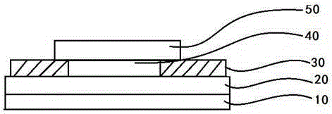
[0022] The high-reliability SMD LED packaging structure described in this embodiment includes a metal base 10, and a voltage-resistant ceramic layer 20 is formed on the metal base, and a metal circuit layer 30 and a high-voltage ceramic layer are formed on the voltage-resistant ceramic layer 20. A thermally conductive ceramic layer 40 ; and an SMD LED lamp bead 50 is arranged on the metal circuit layer 30 and the high thermally conductive ceramic layer 40 . The metal matrix can be metal matrixes such as Al, Cu, Ag and Ni or their alloy matrix; the metal circuit layer is formed by dry etching through a deposited conductive metal layer, and the conductive metal is usually preferably Cu, Ag, Al or their alloy materials. The thickness of the high thermal conductivity ceramic layer is 10-500um; and the high thermal conductivity ceramic layer is preferably AlN, and is formed by a known sintering method. The high thermal conductivity ceramic layer and the pressure-resistant ceramic ...
Embodiment 2
[0024] The high-reliability SMD LED packaging structure described in this embodiment includes a metal base 10, and a voltage-resistant ceramic layer 20 is formed on the metal base, and a metal circuit layer 30 and a high-voltage ceramic layer are formed on the voltage-resistant ceramic layer 20. A thermally conductive ceramic layer 40 ; and an SMD LED lamp bead 50 is arranged on the metal circuit layer 30 and the high thermally conductive ceramic layer 40 . The metal substrate can be aluminum or aluminum alloy substrate; the metal circuit layer is formed by dry etching through the deposited conductive metal layer, and the conductive metal is usually preferably Cu, Ag, Al or their alloy materials . The thickness of the high thermal conductivity ceramic layer is 10-500um; and the high thermal conductivity ceramic layer is preferably AlN, and is formed by a known sintering method. The high thermal conductivity ceramic layer and the pressure-resistant ceramic layer are bonded by ...
PUM
 Abstract
Description
Claims
Application Information
