A method for depositing thick aluminum-copper film layers

A thin-film, aluminum-copper technology, applied in coating, metal material coating process, ion implantation plating, etc., can solve the problems of reducing the service life of semiconductor equipment, temperature rise, wafer temperature rise, etc., to avoid temperature The effect of increasing, reducing whisker-like defects and increasing service life

Active Publication Date: 2016-03-09
SHANGHAI HUAHONG GRACE SEMICON MFG CORP
View PDF5 Cites 0 Cited by
  • Summary
  • Abstract
  • Description
  • Claims
  • Application Information

AI Technical Summary

Problems solved by technology

However, when the reaction chamber is used to continuously deposit Al-Cu thin films on different wafers, working in a high-temperature and high-pressure environment for a long time will make the temperature of various components in the reaction chamber (including shielding layer, ring and base, etc.) further increase. As a result, the temperature of the wafer currently being deposited in the reaction chamber continues to rise, and eventually the whisker-shaped defects formed on the surface of the aluminum-copper film become more and more serious, and its semiconductor performance cannot be guaranteed.
[0005] At the same time, the deposition process used in the prior art will also cause the reaction chamber and its internal components to be damaged due to long-term exposure to the harsh environment of high temperature and high pressure, reducing the service life of semiconductor equipment

Method used


Image

  • A method for depositing thick aluminum-copper film layers
  • A method for depositing thick aluminum-copper film layers

Examples


Embodiment 1

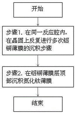
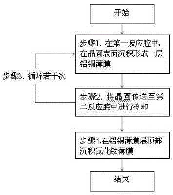
[0039] In the first embodiment, it is necessary to deposit an aluminum-copper thin film layer with a thickness of 40K on the wafer, and the specific operation steps are as follows:

[0040] Step 1. In the first PVD reaction chamber, a first layer of aluminum-copper film with a thickness of 8000 Å is deposited on the surface of the wafer by PVD method;

[0041] Step 2, transferring the wafer deposited with the first layer of Al-Cu thin film to the second PVD reaction chamber, and cooling at room temperature for 20 seconds;

[0042] Step 3. Transfer the cooled wafer to the first PVD reaction chamber again, and continue to perform the deposition process and cooling process 4 times (that is, a total of 5 cycles), and deposit the second layer to the first layer on the wafer in turn. Five-layer aluminum-copper film, and after completing the deposition step of a layer of 8000 ? Aluminum-copper film layer;

[0043] Step 4, depositing a TiN film on top of the 40K?Al-Cu film layer.

Embodiment 2

[0045] In the second embodiment, it is necessary to deposit an aluminum-copper thin film layer with a thickness of 36K on the wafer, and the specific operation steps are as follows:

[0046] Step 1. In the first PVD reaction chamber, a first layer of aluminum-copper film with a thickness of 6000 Å is deposited on the surface of the wafer by PVD method;

[0047] Step 2, transfer the wafer on which the first layer of Al-Cu film has been deposited to the second PVD reaction chamber, and cool it at 30° C. for 15 seconds;

[0048]Step 3. Retransmit the cooled wafer to the first PVD reaction chamber, and continue to cycle through the deposition process and cooling process for 5 times (that is, a total of 6 cycles), and deposit the second layer to the first layer on the wafer in turn. Six-layer aluminum-copper film, and after each deposition of a layer of 6000? ?Aluminum-copper film layer;

[0049] Step 4, depositing a TiN film on top of the 36K?Al-Cu film layer.

Embodiment 3

[0051] In the third embodiment, it is necessary to deposit an aluminum-copper thin film layer with a thickness of 20K on the wafer, and the specific operation steps are as follows:

[0052] Step 1. In the first PVD reaction chamber, a first layer of aluminum-copper film with a thickness of 4000 Å is deposited on the surface of the wafer by PVD method;

[0053] Step 2, transfer the wafer on which the first layer of Al-Cu film has been deposited to the second PVD reaction chamber, and cool it at 40° C. for 12 seconds;

[0054] Step 3. Transfer the cooled wafer to the first PVD reaction chamber again, and continue to perform the deposition process and cooling process 4 times (that is, a total of 5 cycles), and deposit the second layer to the first layer on the wafer in turn. Five-layer aluminum-copper film, and after each deposition step of a 4000? ?Aluminum-copper film layer;

[0055] Step 4, depositing a TiN film on top of the 32K?Al-Cu film layer.


PUM


Abstract

The invention relates to a method for depositing a thick aluminum-copper film layer with thickness bigger than and equal to 10KA. The method comprises the following steps: a step 1 of depositing on a water surface to form a aluminum-copper film layer in a first reaction cavity; a step 2 of transmitting the water deposited with the aluminum-copper film to a second reaction cavity for cooling, wherein the temperature in the second reaction cavity is lower than that in the first reaction cavity; a step 3 of transmitting the cooled wafer in the first reaction cavity, carrying out the depositing process in the step 1 and the cooling process in the step 2 in a circulating manner to deposit a plurality of layer of aluminum-copper films on the wafer in sequence, and transmitting the wafer in the second reaction cavity for cooling until the thickness of the deposited aluminum-copper films reaches a target value after completing the depositing step of one aluminum-copper film layer every time; and a step 4 of depositing a titanium nitride film on the top of the aluminum-copper film layer. According to the method for depositing the thick aluminum-copper film layer disclosed by the invention, the depositing step and the cooling step are carried out in the circulating manner, so that the wafer temperature is prevented from being extremely high; moreover, the generation of crystal whiskers on the surface of the aluminum-copper film layers is effectively inhibited.

Description

technical field [0001] The invention belongs to the technical field of semiconductor manufacturing, and relates to a method for depositing a metal layer, in particular to a deposition method for a thick aluminum-copper thin film layer, which can reduce the whiskers formed on the surface of the aluminum-copper thin film layer during the deposition process . Background technique [0002] In the field of semiconductors, thick aluminum-copper films with a thickness greater than 10K? (kiloangstroms) generally have low sheet resistance, so the thick aluminum-copper films are essential in the application of semiconductor radio frequency (RF) devices and power devices. However, compared with the ordinary aluminum-copper film whose thickness is in the range of 2000? to 8000?, whisker-like defects will be generated on the surface of the thick aluminum-copper film during the continuous deposition process. Moreover, for thicker aluminum-copper films, the problem of whisker-like defects...

Claims


Application Information

Patent Timeline
Patent Type & Authority Patents(China)
IPC IPC(8): C23C14/54C23C14/16H01L21/02H01L21/3205
Inventor 赵波
Owner SHANGHAI HUAHONG GRACE SEMICON MFG CORP
Why Eureka
Try Eureka