
COB (Chip on Board) packaged LED (Light-Emitting Diode) module and manufacturing process thereof

A technology of LED module and manufacturing process, which is applied in household, office lighting, and commercial fields, can solve the problems of cost reduction and light color consistency, and achieve the effects of reducing production costs, ensuring light color consistency, and improving reflectivity

Active Publication Date: 2013-10-23
HANGZHOU HPWINNER OPTO CORP
View PDF8 Cites 9 Cited by
  • Summary
  • Abstract
  • Description
  • Claims
  • Application Information

AI Technical Summary

Problems solved by technology

[0006] The purpose of the present invention is to provide a COB-packaged LED module and its manufacturing process. On this basis, the LED with this structure can achieve the ultimate light output efficiency, reduce the cost, and solve the problem of difficult light color consistency.

Method used


Image

  • COB (Chip on Board) packaged LED (Light-Emitting Diode) module and manufacturing process thereof
  • COB (Chip on Board) packaged LED (Light-Emitting Diode) module and manufacturing process thereof
  • COB (Chip on Board) packaged LED (Light-Emitting Diode) module and manufacturing process thereof

Examples


Embodiment 1

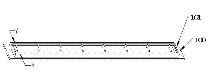
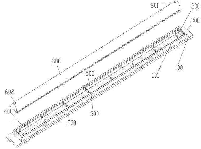
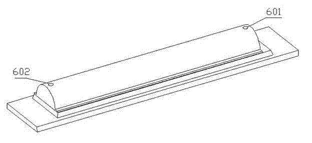
[0050] figure 1 It is a schematic diagram of the aluminum substrate after injection molding of the present invention; figure 2 It is a schematic diagram of the structure of the lens of the present invention opened; image 3 It is a schematic diagram of the external structure of the present invention; Figure 4 for figure 1 A cross-sectional view of the A-A direction.

[0051] Please refer to Figure 1 to Figure 4 , a COB packaged LED module, including an aluminum substrate 100, eight LED chips 200, an optical lens group, sixteen gold wires 300, eight solid crystal positions (not shown in the figure) and sixteen welding pads 500. The shape of the aluminum substrate 100 is rectangular, and the optical lens group preferably includes an optical lens 600 .

[0052]Wherein, the eight LED chips 200 are arranged on the upper surface of the aluminum substrate 100, the optical lens 600 is arranged on the top of the aluminum substrate 100, the optical lens 600 covers all the LED c...

Embodiment 2

[0069] The difference between Embodiment 2 and Embodiment 1 is that the fluorescent adhesive layer 400 is not arranged on the LED chip 200, the phosphor particles are far away from the LED chip 200, and are not in direct contact with the LED chip 200. In Embodiment 2, the fluorescent adhesive layer 400 is set On the optical lens 600 , specifically, the fluorescent glue layer 400 is disposed on the inner surface of the optical lens 600 .

[0070] Since the phosphor is excited by the blue light chip with a low wavelength, the phosphor itself will also have heat after excitation, and the heat of the chip itself will form a superposition of heat. If the phosphor is kept away from the LED chip, the heat will not be superimposed. The heat dissipation effect is good, which can prolong the service life. At the same time, the fluorescent powder is located on the inner surface of the lens or inside the lens body, so that the light is more uniform and the light effect is good.

[0071] ...

Embodiment 3

[0089] The difference between Embodiment 3 and Embodiment 1 is that the fluorescent adhesive layer 400 is not arranged on the LED chip 200, the phosphor particles are far away from the LED chip 200, and are not in direct contact with the LED chip 200. In Embodiment 3, the fluorescent adhesive layer 400 is set On the optical lens 600, specifically, the phosphor particles are mixed in the material for making the optical lens 600 (that is, the body of the optical lens 600 is mixed with phosphor), and the fluorescent adhesive layer 400 and the optical lens 600 are set as an integrated structure. for one.

[0090]The difference between Embodiment 3 and Embodiment 2 is that in Embodiment 2, the fluorescent adhesive layer 400 is arranged on the inner surface of the optical lens 600, and in Embodiment 3, phosphor particles are mixed in the material for making the optical lens 600 (that is, The body of the optical lens 600 is mixed with fluorescent powder), and the fluorescent glue lay...


PUM


Abstract

The invention provides a COB packaged LED module and a manufacturing process thereof. The module comprises an aluminum substrate, an optical lens group and LED chips arranged on the upper surface of the aluminum substrate. The optical lens group comprises at least one optical lens which is a column-shaped one. The optical lens group is arranged above the aluminum substrate and covers all the LED chips inside the same glue housing. Transparent colloid is filled inside the optical lens. The transparent colloid filled inside the optical lens enables the LED module filled with the transparent colloid to effectively improve the light extraction efficiency due to the fact that the refractive index of the transparent colloid is higher than that of the air. Meanwhile, the transparent colloid is covered by the whole LED module. The photochromic consistency is ensured. The production yield rate is increased while the production cost is lowered.

Description

technical field [0001] The invention relates to a COB packaging technology for LEDs, in particular to a COB packaged LED module and a manufacturing process thereof, which are used in household, commercial, office lighting and other fields. [0002] Background technique [0003] In recent years, with the rapid development of LED technology and the introduction of bans on the sale of incandescent lamps in various countries, LED lights, a new type of energy with advantages such as energy saving, environmental protection, and long life, have gradually entered the fields of household, commercial, and office lighting. [0004] At present, in order to meet the needs of various fields, LED packaging forms are becoming more and more diversified. LED COB packaging is one of them, but the current LED COB packaging is still incomplete. For example, the application number is 201020559389.0, and the application date is The patent document published on 2010.09.28 and published on 2011.04....

Claims


Application Information

Patent Timeline
Patent Type & Authority Applications(China)
IPC IPC(8): H01L33/58H01L33/48
Inventor 吕华丽
Owner HANGZHOU HPWINNER OPTO CORP
Learn More