Organic electroluminescence device and manufacturing method thereof

An electroluminescent device and electroluminescent technology, which are applied in the direction of electric solid device, semiconductor/solid state device manufacturing, electrical components, etc., can solve the problems of low luminous efficiency of the device, affect the luminous efficiency, light loss, etc., and improve the front luminous intensity. , The effect of improving light extraction efficiency and improving light extraction rate

Inactive Publication Date: 2013-10-23
OCEANS KING LIGHTING SCI&TECH CO LTD +1
View PDF9 Cites 1 Cited by
  • Summary
  • Abstract
  • Description
  • Claims
  • Application Information

AI Technical Summary

Problems solved by technology

[0004] In traditional organic electroluminescent devices, the ITO glass substrate is used as the light-emitting surface. The preparation technology of this device is mature and there are many studies. The absorption and reflection of the glass can finally be emitted into the air, and because the glass surface is relatively flat and the thickness of the glass is relatively large, the optical path is increased, so that more light is refracted to both sides of the glass, causing the glass to exit into the period The probability of the light is reduced, which ultimately affects the luminous efficiency. Therefore, the emission rate of light emitted into the air is very low, and most of the light is lost, making the luminous efficiency of the device low.

Method used


Image

  • Organic electroluminescence device and manufacturing method thereof
  • Organic electroluminescence device and manufacturing method thereof
  • Organic electroluminescence device and manufacturing method thereof

Examples


preparation example Construction

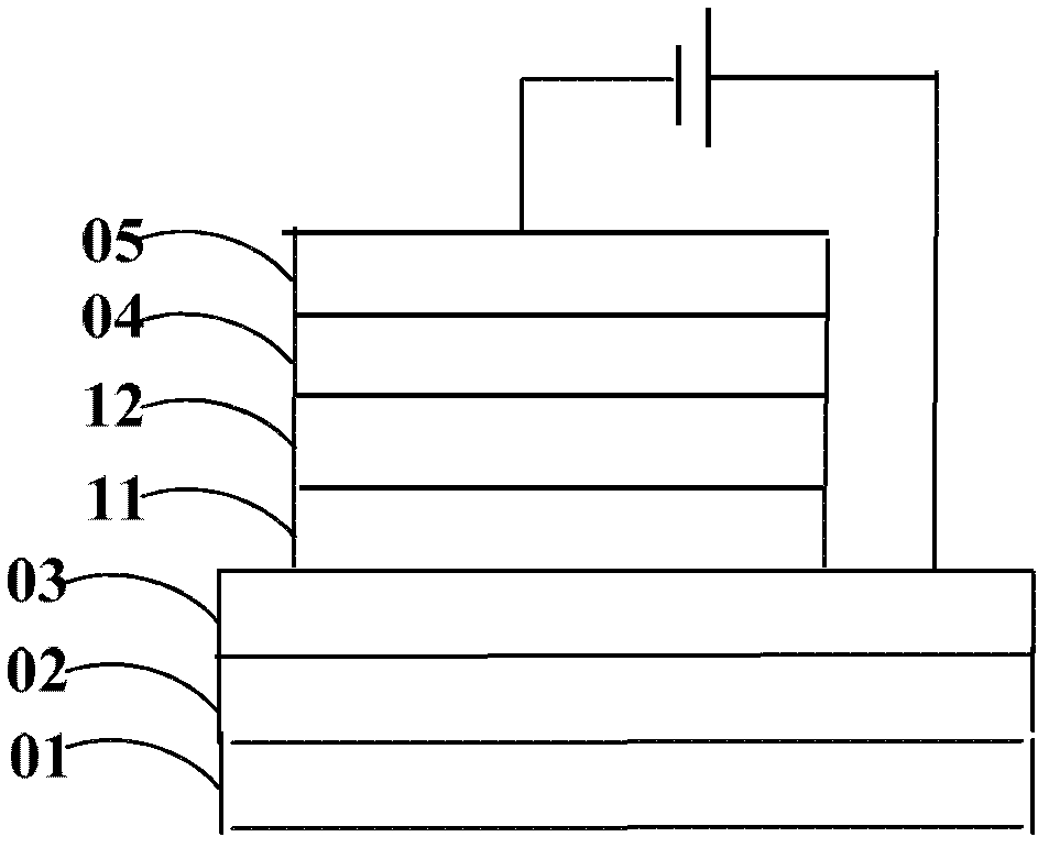
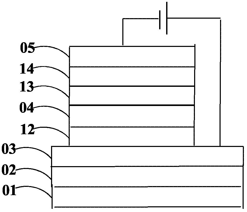
[0035] Another object of the embodiments of the present invention is to provide a method for preparing the above-mentioned organic electroluminescent device, and please refer to Figure 1~4 , which includes the following steps:

[0036] S01: Select a transparent metal oxide with a mass ratio of 0.05-0.6 and a colorless metal compound with a refractive index greater than 2.0, and mix them to obtain a scattering layer material;

[0037] S02: forming a scattering film on the substrate 01 with the scattering layer material to obtain the scattering layer 02;

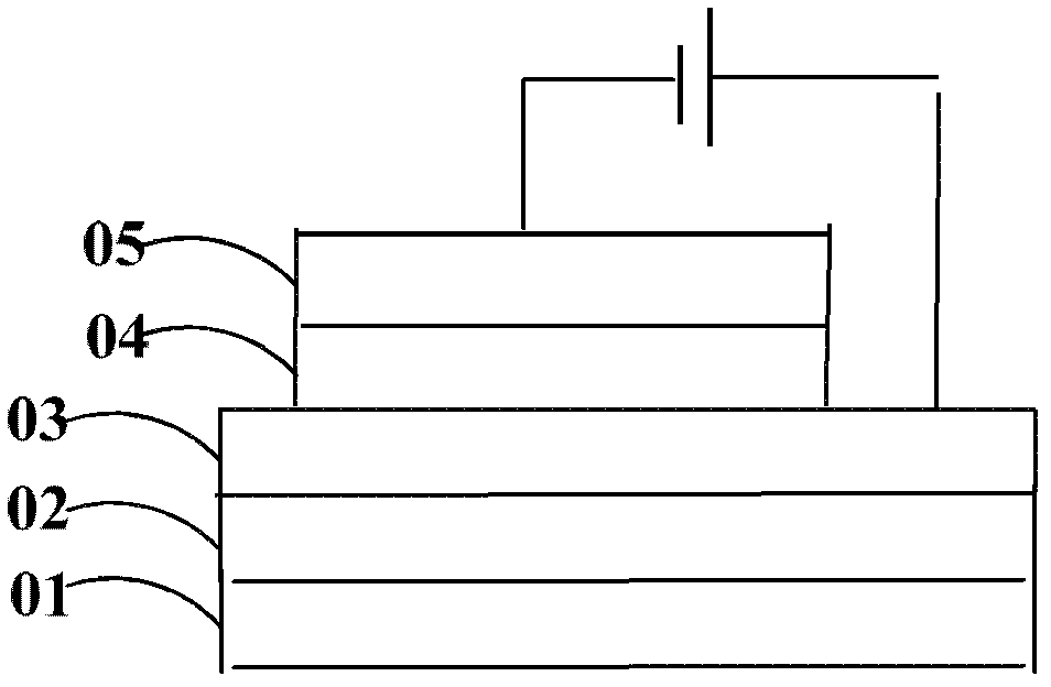
[0038] S03: sequentially preparing an anode layer 03, a light emitting layer 04 and a cathode layer 05 on the scattering layer 02 to obtain the organic electroluminescence device.

[0039] Specifically, the preferred composition and thickness of each layer of the organic electroluminescent device are as described above, and will not be repeated here to save space.

[0040] In step S01, a 20-200 nm transparent metal oxide an...

Embodiment 1

[0045] First, wash the glass substrate with detergent, deionized water, and ultrasonic for 15 minutes to remove organic pollutants on the glass surface; -4 The doped scattering layer was prepared by vapor deposition under Pa vacuum pressure, and the material was MoO 3 :ZnS, MoO 3 The mass ratio to ZnS is 0.25, and the thickness is 300nm; then the anode conductive film is prepared by magnetron sputtering, the material is ITO, and then the hole injection layer MoO is sequentially evaporated 3 , thickness is 40nm; hole transport layer TCTA, thickness is 50nm; light emitting layer Ir(ppy) 3 Doped TPBi(Ir(ppy) 3 The mass ratio to TPBi is 0.1), the thickness is 20nm; the electron transport layer TAZ, the thickness is 60nm; the electron injection layer is CsN 3 , with a thickness of 1 nm; and a cathode Ag layer, with a thickness of 100 nm; an organic electroluminescent device is obtained.

Embodiment 2

[0047] First, the glass substrate is washed with detergent, deionized water, and ultrasonic for 15 minutes to remove organic pollutants on the glass surface; the doped scattering layer is prepared by evaporation on the glass substrate, and the material is WO 3 : ZnSe, WO 3 The mass ratio to ZnSe is 0.05, and the thickness is 500nm; then the anode conductive film is prepared by magnetron sputtering, the material is IZO, and then the hole injection layer is sequentially evaporated, and the material is V 2 o 5 , with a thickness of 20nm; the hole transport layer NPB, with a thickness of 60nm; the light emitting layer Ir(MDQ) 2 (acac) doped TAZ, Ir(MDQ) 2 The mass ratio of (acac) to TAZ is 0.02, the thickness is 20nm; the electron transport layer TPBi, the thickness is 80nm; the electron injection layer Cs 2 CO 3 , with a thickness of 10nm and a metal cathode Au layer with a thickness of 180nm; an organic electroluminescence device is obtained, and its current efficiency is 31...


PUM

PropertyMeasurementUnit
Thicknessaaaaaaaaaa
Thicknessaaaaaaaaaa
Thicknessaaaaaaaaaa

Abstract

The invention discloses an organic electroluminescence device belonging to the field of organic electroluminescence. The organic electroluminescence device comprises a substrate, a scattering layer, an anode layer, a light emitting layer and a cathode layer which are stacked in sequence, wherein a scattering layer material is made of a mixture including transparent metal oxide and a colorless metal compound with the refractive index larger than 2.0 according to the mass rate of 0.05-0.6. The invention also provides a manufacturing method of the organic electroluminescence device. The manufacturing method comprises the following steps of: selecting the transparent metal oxide and the colorless metal compound with the refractive index larger than 2.0 according to the mass rate of 0.05-0.6, and mixing the transparent metal oxide and the colorless metal compound to obtain a scattering layer material; forming a scattering film by the scattering layer material on the substrate to obtain the scattering layer; and sequentially preparing the anode layer, the light emitting layer and the cathode layer on the scattering layer to obtain the organic electroluminescence device. According to the organic electroluminescence device, light inside the device is extracted out by using the scattering layer, so that the light emitting efficiency is enhanced.

Description

technical field [0001] The invention belongs to the field of organic electroluminescence, and in particular relates to an organic electroluminescence device and a preparation method thereof. Background technique [0002] In 1987, C.W.Tang and Van Slyke of Eastman Kodak Company in the United States reported a breakthrough in the research of organic electroluminescence. A high-brightness, high-efficiency double-layer organic electroluminescent device (OLED) was prepared by using ultra-thin film technology. In the device with double-layer structure, the luminance reaches 1000cd / m2 at 10V, the luminous efficiency is 1.51lm / W, and the lifetime is more than 100 hours. [0003] The principle of OLED light emission is based on the action of an external electric field, electrons are injected from the cathode to the lowest unoccupied molecular orbital (LUMO) of organic matter, and holes are injected from the anode to the highest occupied orbital (HOMO) of organic matter. Electrons a...

Claims


Application Information

Patent Timeline
IPC IPC(8): H01L51/52H01L51/54
Inventor 周明杰王平黄辉陈吉星
Owner OCEANS KING LIGHTING SCI&TECH CO LTD
Why Eureka
Try Eureka