A method for forming a silicon germanium source/drain structure
A silicon germanium and silicon germanium layer technology, applied in semiconductor devices and other directions, can solve problems such as device performance deterioration, and achieve the effects of performance improvement, compressive stress assurance, and lattice mismatch reduction.
- Summary
- Abstract
- Description
- Claims
- Application Information
AI Technical Summary
Problems solved by technology
Method used
Image
Examples
Embodiment 1
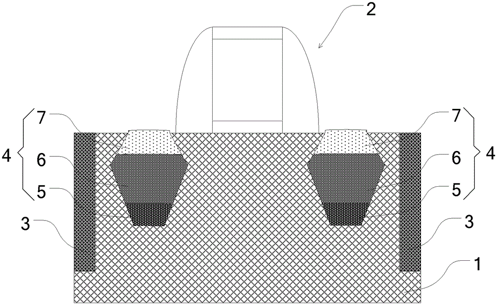
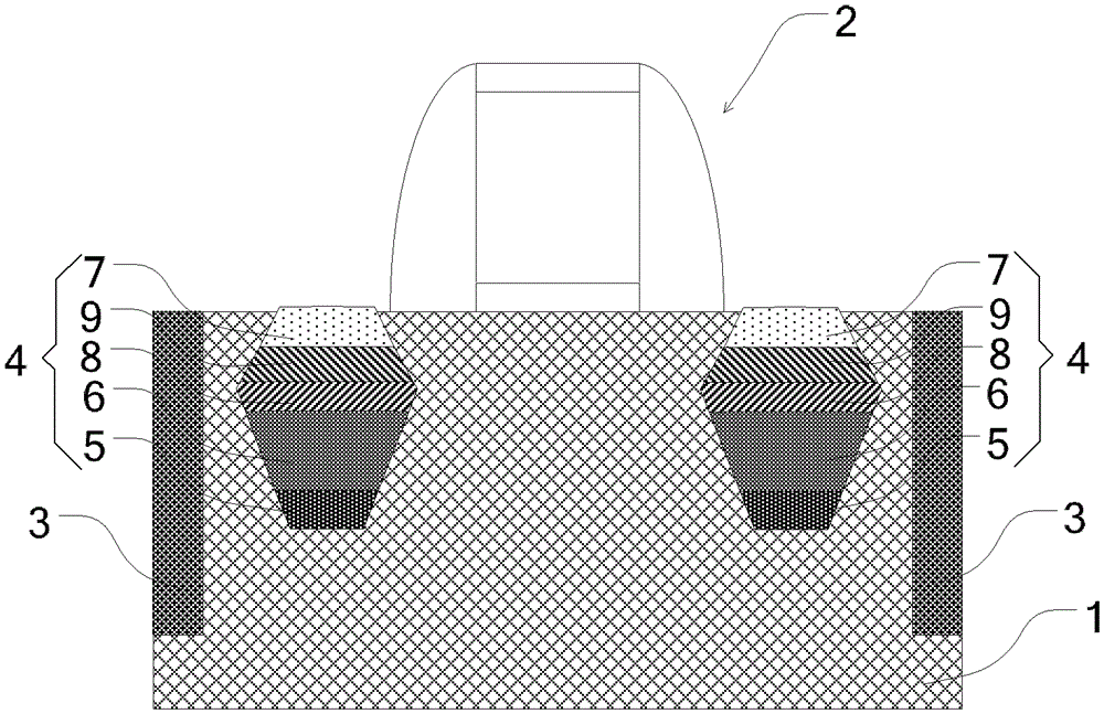
[0050] Please refer to Figure 2a , a formation process of a silicon germanium source / drain structure, providing a substrate 1, such as a silicon substrate, etc., forming a gate structure 2 on the substrate 1, forming an isolation structure 3 in the substrate, etching The substrate 1 forms recesses on both sides of the gate structure 2, and a source / drain region 4 is formed in the recess, wherein the forming of the source / drain region 4 includes: forming a seed layer 5, and the seed layer 5 is A silicon germanium layer, a bulk layer 6 is formed on the seed layer 5, the bulk layer 6 is a silicon germanium layer or a silicon germanium boron layer, a first transition layer 8 is formed on the bulk layer, and the first transition layer 8 A second transition layer 9 is formed on it, and an upper cladding layer 7 is formed on the second transition layer 9 .
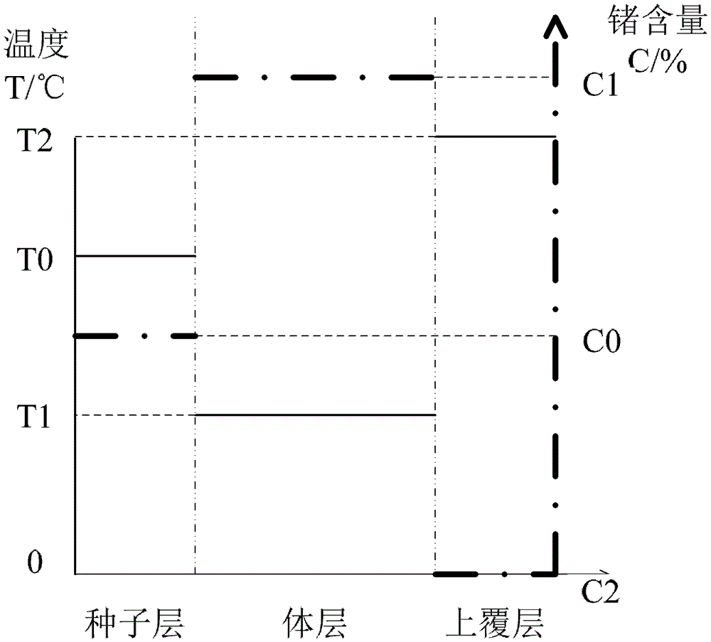
[0051] Specifically, please combine Figure 2b , the content of germanium in the growth process of the first transition laye...
Embodiment 2
[0053] Please refer to Figure 3a , a formation process of a silicon germanium source / drain structure, providing a substrate 1, such as a silicon substrate, etc., forming a gate structure 2 on the substrate 1, forming an isolation structure 3 in the substrate, etching The substrate 1 forms recesses on both sides of the gate structure 2, and a source / drain region 4 is formed in the recess, wherein the forming of the source / drain region 4 includes: forming a seed layer 5, and the seed layer 5 is A silicon germanium layer, a bulk layer 6 is formed on the seed layer 5, the bulk layer 6 is a silicon germanium layer or a silicon germanium boron layer, a transition layer 10 is formed on the bulk layer 6, and an upper layer is formed on the transition layer 10 Cladding 7.
[0054] Specifically, please combine Figure 3b , the transition layer 10 satisfies the following two conditions: 1. The germanium content decreases linearly during the growth process, that is, from the same germa...
PUM
 Abstract
Description
Claims
Application Information


