Metal grid electrode manufacturing method and CMOS manufacturing method

A manufacturing method and metal gate technology, which are applied in the field of metal gate manufacturing and CMOS manufacturing, can solve the problems of semiconductor device failure, open circuit, and reduced conductivity of Al metal electrodes, so as to prevent performance degradation and avoid voids. Effect

Inactive Publication Date: 2013-10-30
SEMICON MFG INT (SHANGHAI) CORP
View PDF8 Cites 7 Cited by
  • Summary
  • Abstract
  • Description
  • Claims
  • Application Information

AI Technical Summary

Problems solved by technology

The appearance of voids leads to a decrease in the conductivity of the Al metal electrode or even an open circuit,

Method used


Image

  • Metal grid electrode manufacturing method and CMOS manufacturing method
  • Metal grid electrode manufacturing method and CMOS manufacturing method
  • Metal grid electrode manufacturing method and CMOS manufacturing method

Examples


Example Embodiment

[0075] In order to make the objectives, technical solutions and advantages of the present invention clearer, the present invention will be further described in detail below with reference to the accompanying drawings and embodiments.

[0076] Such as Figure 5 Shown is a flowchart of an embodiment of a metal gate manufacturing method of the present invention, and the method includes:

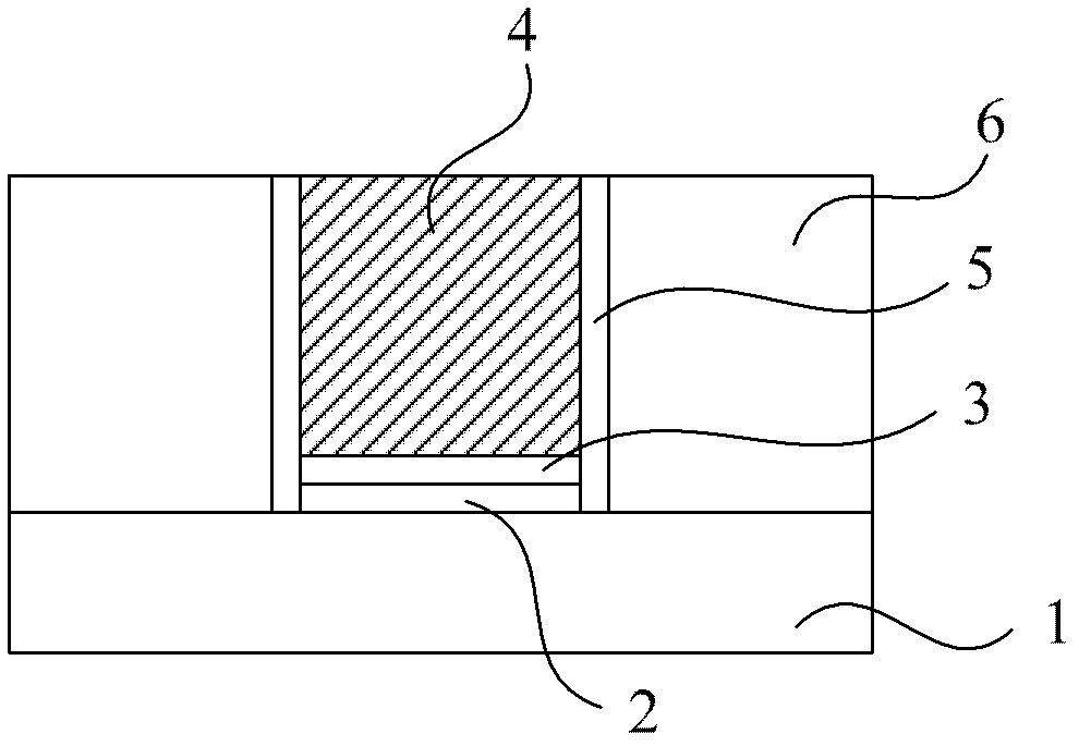
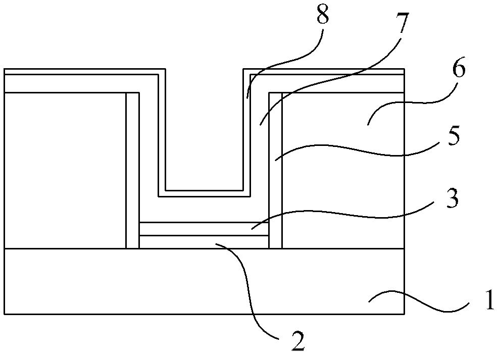
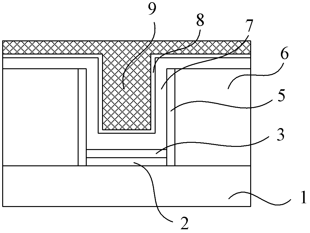
[0077] Step 1: Provide a substrate formed with a dummy gate structure, the dummy gate structure including an interface layer, a high-k gate dielectric layer, and a dummy polysilicon gate sequentially formed on the substrate, along the dummy gate structure Side walls are formed on both sides, and an interlayer dielectric layer is also formed on the substrate outside the side walls;

[0078] Step 2: Remove the dummy polysilicon gate to form a trench, and sequentially deposit a metal work function layer and an isolation layer in the trench;

[0079] Step 3: Deposit a polysilicon layer and fill the trench w...


PUM


Abstract

The invention discloses a metal grid electrode manufacturing method and a CMOS manufacturing method based on the metal grid electrode manufacturing method. The metal grid electrode manufacturing method includes the steps of providing a substrate which is provided with a pseudo grid structure, removing a pseudo polycrystalline silicon grid electrode to form a groove, sequentially depositing a metal work function layer and an isolating layer in the groove, depositing a polycrystalline silicon layer, filling the groove with the polycrystalline silicon layer, depositing an A1 metal layer on the polycrystalline silicon layer, conducting thermal annealing treatment so that the A1 metal layer and the polycrystalline silicon layer can be interchangeable and an A1 electrode can be formed, and removing the replaced polycrystalline silicon layer and A1 metal located outside the groove so that a metal grid electrode can be formed. According to the metal grid electrode manufacturing method and the CMOS manufacturing method, in the manufacturing process of smaller than 32nm, gaps in the A1 electrode can be prevented, and further the performance of semiconductor devices is prevented from being lowered.

Description

technical field [0001] The present invention relates to semiconductor manufacturing technology, in particular to a manufacturing method of a metal gate of a semiconductor device and a CMOS (Complementary Metal-Oxide-Semiconductor, Complementary Metal-Oxide Semiconductor) manufacturing method. Background technique [0002] With the continuous reduction of the feature size (CD, Critical Dimension) in the semiconductor manufacturing process, the high dielectric constant metal gate (HKMG) has replaced the original polysilicon gate, and is generally used in 45nm and 32nm and smaller in the process node of the feature size. The introduction of high dielectric constant metal gates solves the technical obstacles faced by traditional gates, such as reducing EOT (Equivalent Oxide Thickness, equivalent gate oxide thickness) and Vt (threshold voltage), reducing transistor leakage current, etc. In turn, the performance of the semiconductor device is improved. [0003] An existing metho...

Claims


Application Information

Patent Timeline
IPC IPC(8): H01L21/28H01L21/8238
Inventor 平延磊鲍宇肖海波
Owner SEMICON MFG INT (SHANGHAI) CORP
Why Eureka
Try Eureka