Manufacturing method of printed circuit board (PCB) coil and PCB coil

A PCB circuit board and coil technology, applied in the direction of multi-layer circuit manufacturing, containing printed electrical components, etc., can solve the problems of signal interference, uneven winding and uniform distribution of multi-layer coils, and achieve excellent electromagnetic performance and guaranteed parameters The effect of consistency and small parasitic capacitance

Inactive Publication Date: 2013-11-06
UNI TREND TECH (CHINA) CO LTD
View PDF3 Cites 3 Cited by
  • Summary
  • Abstract
  • Description
  • Claims
  • Application Information

AI Technical Summary

Problems solved by technology

[0005] Even if a single-layer coil is wound directly on a smooth bobbin, it is impossible for the winding machine we use now to ensure that the number of turns of the coil is evenly distributed throughout the coil length
In the case of multi-layer winding, the outer coil is wound on the uneven inner coil, and the winding uniformity is more difficult to ensure.
In theory, only completely uniform and symmetrical coils have the best anti-interference ability, so the uneven winding of multi-layer coils will cause signal interference problems

Method used


Image

  • Manufacturing method of printed circuit board (PCB) coil and PCB coil
  • Manufacturing method of printed circuit board (PCB) coil and PCB coil

Examples


Embodiment 1

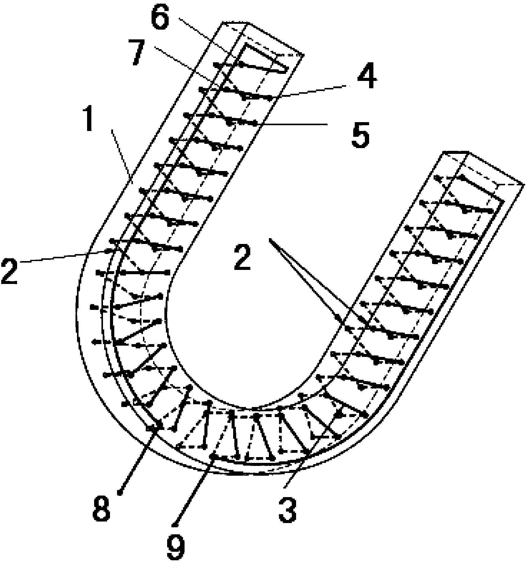
[0032] Embodiment 1: see figure 1 , the present embodiment provides a kind of preparation method of U-shaped PCB coil, and it comprises the following steps:

[0033] (1) Use the electronic design automation EDA software to design the wiring of the PCB coil;

[0034] (2) A single-layer U-shaped double-sided PCB circuit board 1 is set;

[0035] (3) On the U-shaped PCB circuit board 1 described in step (2), a plurality of via holes 2 are arranged, and the inner and outer sides of the via holes 2 are arranged in an orderly manner;

[0036] (4) according to the wiring design of step (1), at the upper surface and the lower surface of U-shaped PCB circuit board 1 described in step (2), carry out etching wiring respectively;

[0037] (5) Fill conductive material in the via hole 2 described in step (3), and the via hole electrically connects the double-sided PCB circuit board through electroplating copper plating, so that the upper and lower copper wires 3 are electrically connected;...

Embodiment 2

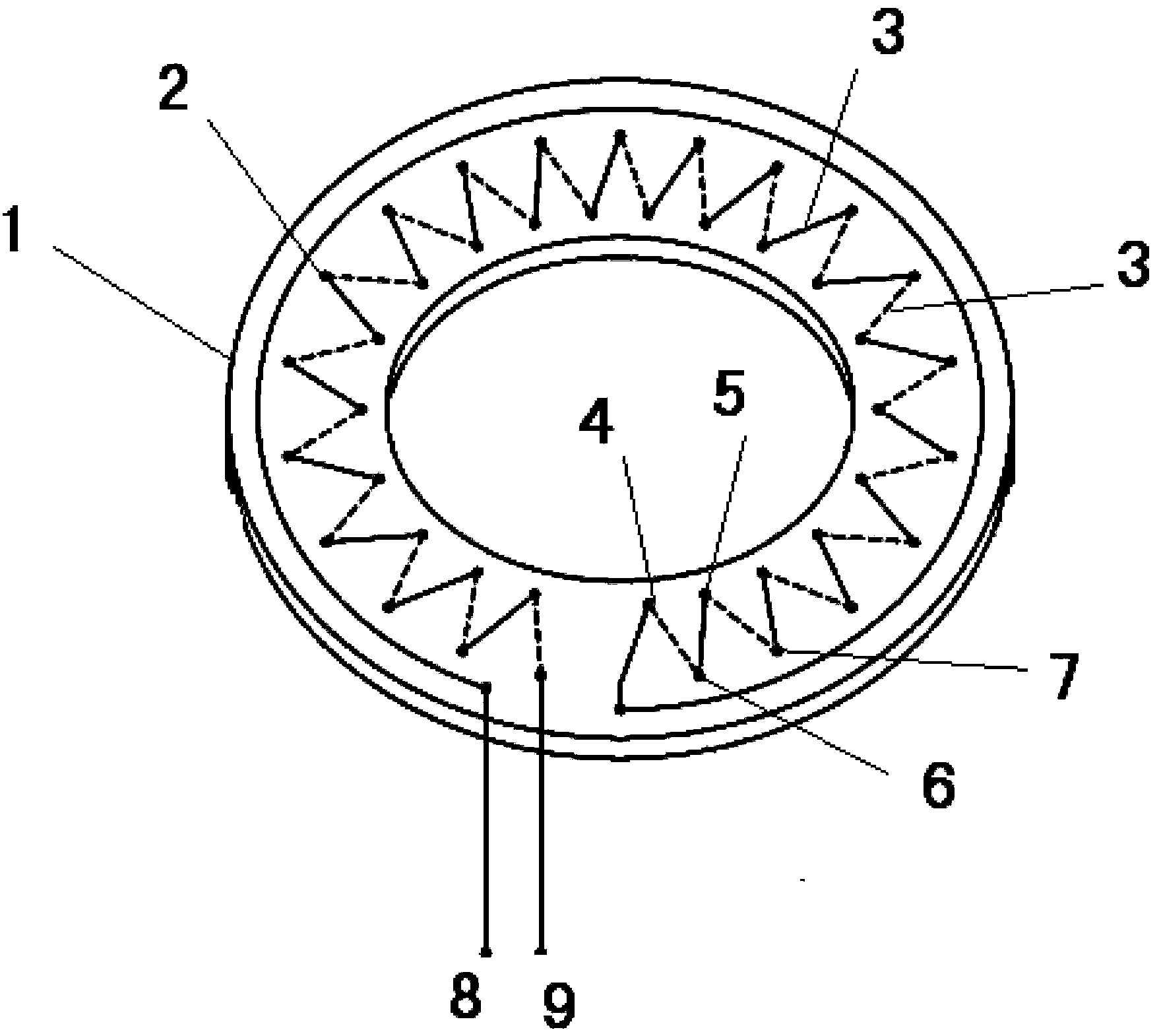
[0049] Example 2: see figure 2 , the preparation method of the ring-type PCB coil and the ring-type PCB coil provided in this embodiment, its steps and composition are basically the same as in Example 1, the difference is that:

[0050] A kind of preparation method of annular PCB coil, it comprises the following steps:

[0051](1) Use the electronic design automation EDA software to design the wiring of the PCB coil;

[0052] (2) A single-layer annular double-sided PCB circuit board 1 is set;

[0053] (3) On the annular PCB circuit board 1 described in step (2), a plurality of via holes 2 are set, and the inner and outer sides of the via holes 2 are arranged in an orderly manner;

[0054] (4) according to the wiring design of step (1), on the upper surface and the lower surface of the annular PCB circuit board 1 described in step (2), carry out etching wiring respectively;

[0055] (5) Fill conductive material in the via hole 2 described in step (3), and the via hole elect...


PUM


Abstract

The invention discloses a manufacturing method of a printed circuit board (PCB) coil. The manufacturing method is characterized by comprising the following steps that (1) wiring design is conducted on the PCB coil by using electronic design automation (EDA) software; (2) a single-layer double-faced PCB is arranged; (3) a plurality of via holes are formed in the PCB of the step (2), and the inner sides and the outer sides of the via holes are distributed orderly in a double-row mode; (4) according to the wiring design of the step (1), etching wiring is conducted on the upper surface and the lower surface of the PCB of the step (2); (5) conductive materials are filled in the via holes of the step (3), the double-faced PCB is electrically connected through the via holes through electroless copper plating so that upper copper wires and lower copper wires are electrically connected; (6) protective layer rosin water is coated on the surfaces of wires arranged in the step (4), after the rosin water is condensed, the PCB coil is obtained. The invention further discloses the PCB coil prepared through the method.

Description

technical field [0001] The invention relates to the technical field of electromagnetic components, in particular to a method for preparing a PCB coil and a PCB coil prepared by implementing the method. Background technique [0002] Traditional transformer coils are generally composed of enameled wires wound on rigid iron cores, non-magnetic skeletons or flexible hoses. In order to increase the mutual inductance coefficient and increase the induced voltage, generally when winding the coil, multiple layers of enameled wire are wound back and forth on the skeleton to increase the number of turns of the coil. Such an approach would cause the following problems: [0003] The cross-sectional area and wire length of each coil are not uniform. The innermost coil is wound directly on the bobbin, so the cross-sectional area of ​​the innermost coil is the cross-sectional area of ​​the bobbin. The outer coil is wound on the basis of the inner coil, so the thickness of the inner coil ...

Claims


Application Information

Patent Timeline
Patent Type & Authority Applications(China)
IPC IPC(8): H05K3/46H05K1/16
Inventor 赵辉罗友文侯孝刚
Owner UNI TREND TECH (CHINA) CO LTD
Why Eureka
Try Eureka