Light-emitting diode with dual-function electrodes and manufacturing method thereof

A light-emitting diode, dual-function technology, applied in circuits, electrical components, semiconductor devices, etc., can solve the problems of low current, difficulty in making vertical electrodes on chips, congestion, etc., to reduce chip voltage, improve chip performance, and increase chip brightness Effect

Active Publication Date: 2013-11-13
EPITOP PHOTOELECTRIC TECH
View PDF3 Cites 2 Cited by
  • Summary
  • Abstract
  • Description
  • Claims
  • Application Information

AI Technical Summary

Problems solved by technology

[0004] Since the base sapphire for making blue-ray chips is non-conductive, it is difficult to make vertical electrodes based on the chip made on the sapphire substrate, so it is very easy to cause low mobility of electrons and holes inside the chip and current congestion.

Method used


Image

  • Light-emitting diode with dual-function electrodes and manufacturing method thereof
  • Light-emitting diode with dual-function electrodes and manufacturing method thereof
  • Light-emitting diode with dual-function electrodes and manufacturing method thereof

Examples


Embodiment Construction

[0019] The specific implementation of a light-emitting diode with dual-function electrodes and its manufacturing method provided by the present invention will be described in detail below in conjunction with the accompanying drawings.

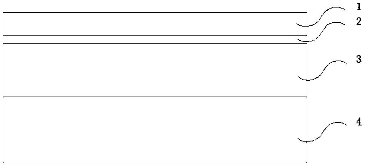
[0020] Reference attached figure 1 , grow a light-emitting structure on the sapphire substrate 4 and deposit it on the sapphire substrate 4 by epitaxial growth (such as MOCVD). The material of the light-emitting structure is a semiconductor material, such as gallium nitride-based compound. Taking GaN material as an example, the light emitting structure includes n-GaN layer 3 , quantum well light emitting layer 2 , and p-GaN layer 1 . The sapphire substrate 4 in this step can also be replaced by other substrates, such as SiC or the like.

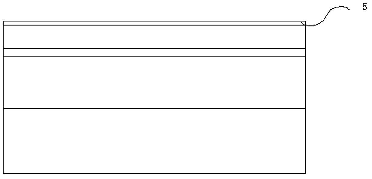
[0021] Reference attached figure 2 , grow the insulating layer 5 by processes such as plasma-enhanced chemical vapor deposition, and the material of the insulating layer 5 can be, for example, silicon oxid...


PUM


Abstract

The invention provides a light-emitting diode with dual-function electrodes, which comprises a substrate, and an N-shaped semi-conductor layer, an active layer and a P-shaped semi-conductor layer that are arranged on the front side of the substrate in sequence, and further comprises a front side P-shaped electrode, a front side N-shaped electrode, a back side electrode and a side electrode; the front side P-shaped electrode is arranged on the surface of a P-shaped semi-conductor substrate; the front side N-shaped electrode is arranged on the surface of an N-shaped semi-conductor substrate; the back side electrode and the side electrode wrap the back side and the side of the substrate; the side of the N-shaped semi-conductor layer is in contact with the front side N-shaped electrode to take a effect of increasing the current of the light-emitting diode. The light-emitting diode has the advantages of effectively improving the chip brightness, reducing the chip voltage and improving the chip performance.

Description

technical field [0001] The invention relates to the manufacture of a light-emitting diode, which belongs to the technical manufacture field of semiconductor devices. Background technique [0002] The core basic structure of a light-emitting diode (LED) includes a p-type semiconductor layer, an active layer (light-emitting layer) and an n-type semiconductor layer. When the LED is subjected to forward bias, the holes in the p region move to the n region, the electrons in the n region move to the p region, and the electrons and holes recombine in the active layer. Theoretically, most of the energy released by the recombination of electrons and holes is released in the form of light (radiative transition). It can be seen that LED can directly convert electrical energy into light energy, so it has the advantages of high energy conversion efficiency and small size. At the same time, because the LED does not contain toxic and harmful substances, it meets the requirements of envir...

Claims


Application Information

Patent Timeline
Patent Type & Authority Applications(China)
IPC IPC(8): H01L33/38
Inventor 徐琦康建郑远志陈向东李晓莹
Owner EPITOP PHOTOELECTRIC TECH
Why Eureka
Try Eureka