Optical gate switch

A technology of optical gate switch and optical waveguide, which is applied in optics, nano optics, nonlinear optics, etc., can solve the problems of large size and gate switch instability, and achieve high stability

Inactive Publication Date: 2013-11-13
NAT INST OF ADVANCED IND SCI & TECH
View PDF6 Cites 2 Cited by
  • Summary
  • Abstract
  • Description
  • Claims
  • Application Information

AI Technical Summary

Problems solved by technology

[0003] The size of the interferometer of the optical gate switch of the space optical system type is large, so the instability of the gate switch operation becomes a problem

Method used


Image

  • Optical gate switch
  • Optical gate switch
  • Optical gate switch

Examples


no. 1 example

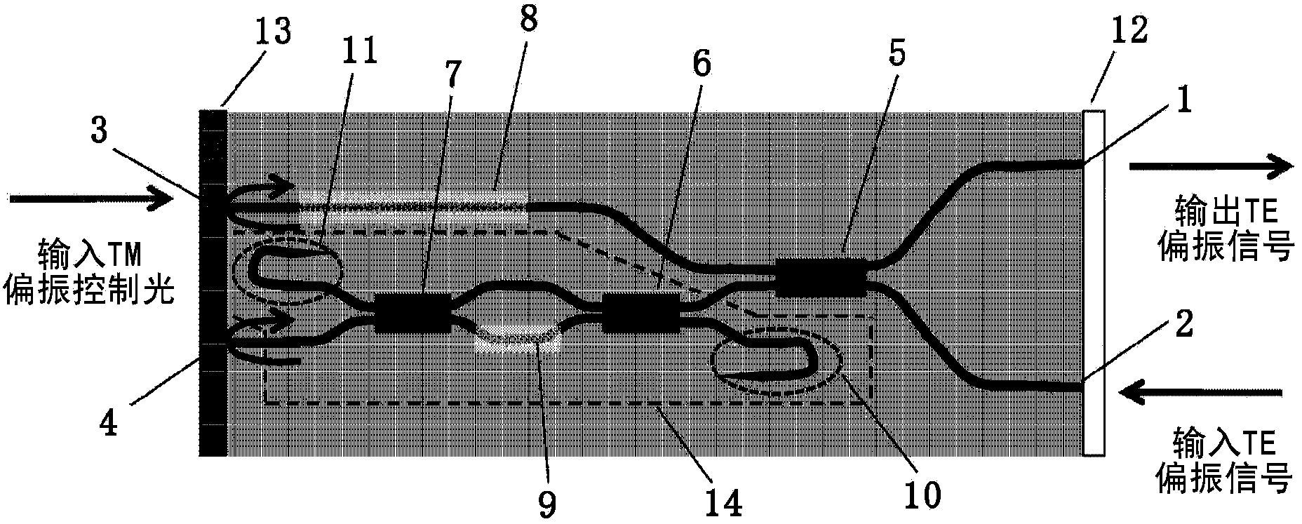
[0063] A preferred embodiment for forming a monolithically integrated shutter switch will be described.

[0064] In order to facilitate the growth of a quantum well structure that produces a phase modulation effect due to interband transitions, an InP substrate is used as a wafer for forming an optical integrated circuit.

[0065] After growing the InP buffer layer on the InP substrate by the molecular beam epitaxy method, it is further grown so that the number of periods of growth is suitable for the InGaAs / AlAsSb coupled double quantum well structure disclosed in detail (S.Gozu et al., Applied Physics Express , 2, 042201-1-3 (2009).) or indicates the thickness required for the quantum well structure equal to or greater than the phase modulation effect of the quantum well to function as a waveguide, after which, the upper part with a thickness of 1 μm is grown again cladding. As a material of the upper cladding layer, any one of InP, InAlAs, and GaAlAsSb is used. The multi-...

no. 2 example

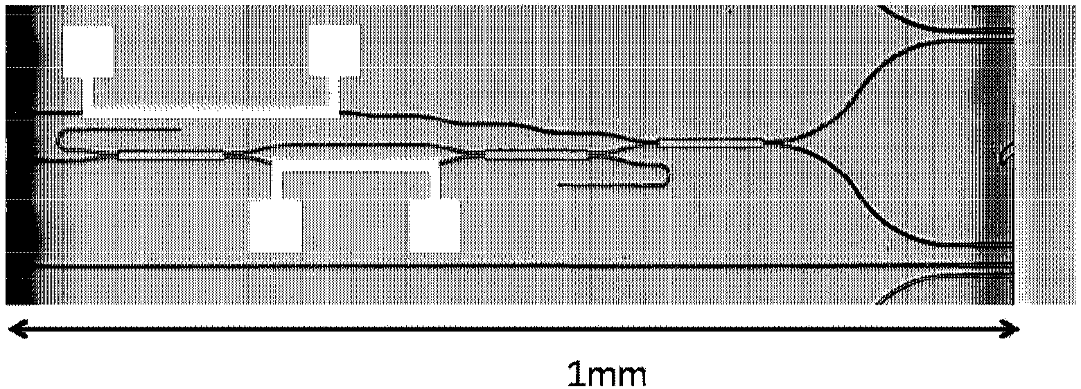
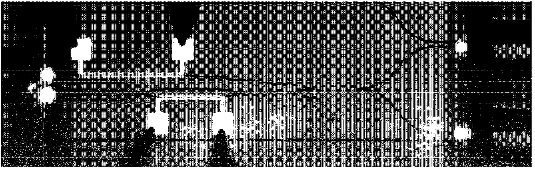
[0094] In the second embodiment, an improvement is made on the basis of the basic structure of the first embodiment, that is, the propagation loss of the element is reduced for TE polarized signal light. refer to Figure 7 to explain. Figure 7 In the basic configuration diagram (see FIG. 1 ) of the present invention, a configuration for reducing loss of signal light in waveguides other than the phase modulator is shown. By phosphorus ion implantation and rapid thermal annealing, to make Figure 7 Quantum well mixing occurs outside the region of the phase modulation section 15 . The structure of the second embodiment is produced by the same method as that of the first embodiment, however, it is different in the following process. Using SiO 2 For example, a mask is formed on a region corresponding to the phase modulation portion 15 on a wafer used for fabrication of an optical integrated circuit. Next, for example, a dose of 1×10 14 ~1×10 15 / cm 2 P or As ions. The ene...


PUM

PropertyMeasurementUnit
refractive indexaaaaaaaaaa

Abstract

The present invention addresses the problem of implementing a monolithic integrated type of optical gate switch which can be reduced in size by integration and can avoid the problem of optical coupling loss of an interferometer optical circuit unit and a phase modulation unit. The optical gate switch of the present invention comprises: an optical waveguide wafer the core layer of which comprises quantum wells showing a phase modulation effect produced by transitions between sub-bands; a Michelson interferometer formed on the optical waveguide wafer; and a variable optical intensity attenuation unit which adjusts the optical balance of the interferometer in one arm on the reflection side of the Michelson interferometer.

Description

technical field [0001] The present invention relates to an optical gate switch. Background technique [0002] It was found that if the TM polarized light is used to photoexcite the subband transition of the InGaAs / AlAsSb semiconductor quantum well, a phase modulation effect with a response speed of several picoseconds will be produced relative to the TE polarized light without absorption loss (refer to the non-patent literature 1). The inventors of the present invention reported an ultra-high-speed optical gate switch using the phase modulation effect described above (see Non-Patent Document 2). Among the shutter switches described above, there is a form of a Mach-Zehnder interferometer of the space optical system type constituted by combining optical components having an angular size ranging from several mm to about 1 cm, such as mirrors and polarizing beam splitters. An optical waveguide including a quantum well exhibiting a phase modulation effect is introduced into an ...

Claims


Application Information

Patent Timeline
Patent Type & Authority Applications(China)
IPC IPC(8): G02F1/365G02F1/017
CPCG02F2001/01733G02F2001/01775G02F2001/215G02F2001/212G02F1/01708G02F2203/48G02F1/2257B82Y20/00G02F1/01733G02F1/01775G02F1/212G02F1/215
Inventor 秋本良一牛头信一郎物集照夫石川浩
Owner NAT INST OF ADVANCED IND SCI & TECH
Why Eureka
Try Eureka