Biomedical electrode with surface micro-structure array and manufacturing method thereof
A microstructure array, biomedical technology, applied in applications, medical science, sensors, etc., can solve the problems of poor repeatability, inaccurate measurement results, unsuitable for long-term use, etc., achieve moderate production costs, expand the scope of use, and process Effects with low equipment requirements
- Summary
- Abstract
- Description
- Claims
- Application Information
AI Technical Summary
Problems solved by technology
Method used
Image
Examples
Embodiment 1
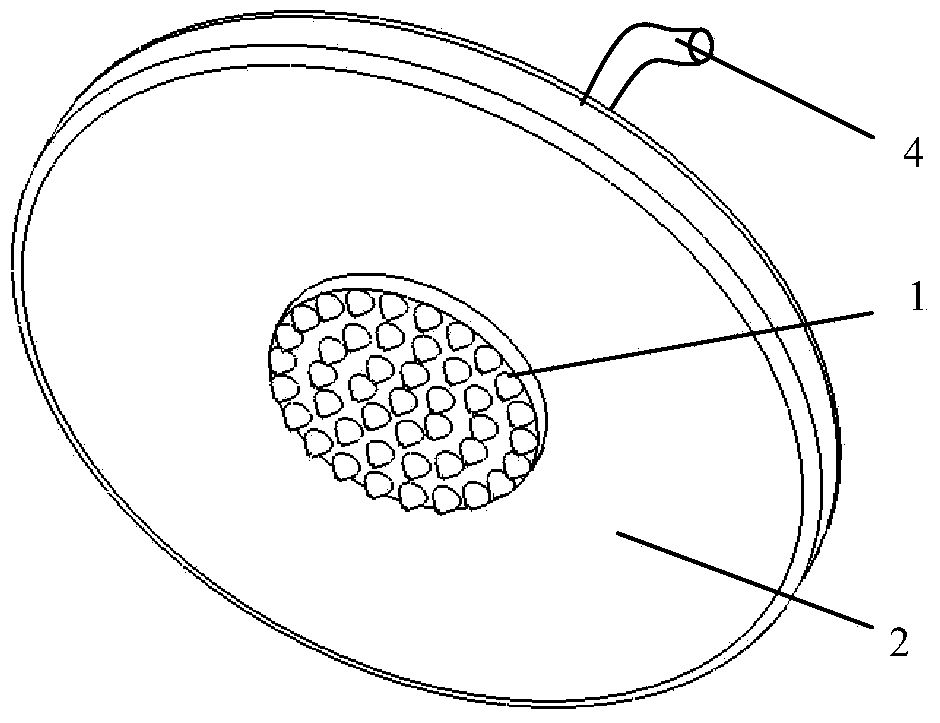
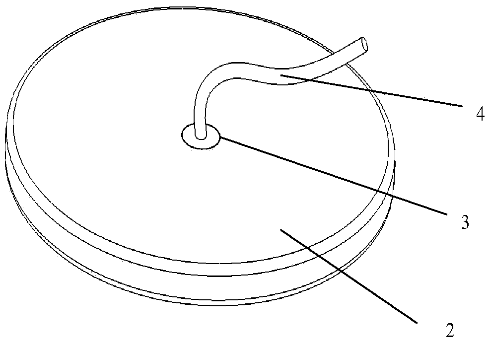
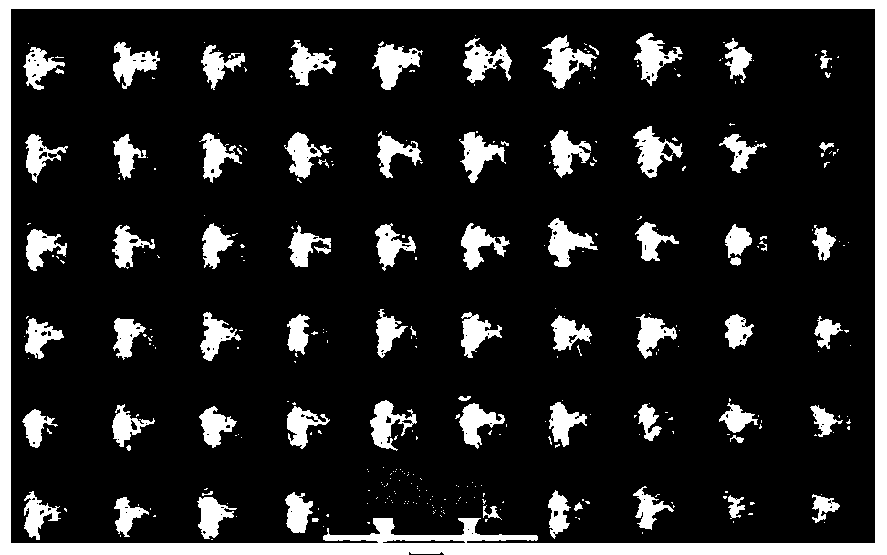
[0027] Such as Figure 1~3 As shown, a biomedical electrode with surface microstructure array characteristics includes four parts: metal electrode core 1 , foam material backing 2 , conductive silver glue 3 and shielding wire 4 . The metal electrode core 1 is pasted on the other side of the foam material backing 2, such as figure 1 shown. The foam backing material 2 and the shielded wire 4 realize the solderless connection through the conductive silver glue 3, such as figure 2 shown. The surface of the metal electrode core has surface cone-like microstructure array features, such as image 3 shown.
[0028] The manufacturing process method includes the following steps:
[0029] The first step is laser processing. Copper metal flakes are selected as the raw material of the metal electrode core. By designing the laser processing route and using laser micromachining technology, a linear array with a vertical and horizontal spacing of 0.1mm×0.1mm conical surface microstruct...
Embodiment 2
[0036] The raw material of the electrode core in the first step can be selected as a metal aluminum sheet material, and a linear array of columnar microstructures with a vertical and horizontal spacing of 0.2mm×0.2mm can be formed by laser processing. Others are the same as in Example 1.
Embodiment 3
[0038] The raw material of the electrode core in the first step can be selected as a stainless steel sheet material, and a linear array of circular microstructures with a vertical and horizontal spacing of 0.3mm×0.3mm can be formed by laser processing. Others are the same as in Example 1.
PUM
| Property | Measurement | Unit |
|---|---|---|
| distance | aaaaa | aaaaa |
| thickness | aaaaa | aaaaa |
Abstract
Description
Claims
Application Information


