Fine spacing laminated packaging structure containing copper pillar and packaging method

A stacked packaging and fine-pitch technology, which is applied to semiconductor/solid-state device components, semiconductor devices, electrical components, etc., can solve the problems of high cost and high cost of electroplating, achieve high production efficiency, omit complex processes, and simple production Effect

Inactive Publication Date: 2013-11-20
NAT CENT FOR ADVANCED PACKAGING CO LTD
View PDF4 Cites 14 Cited by
  • Summary
  • Abstract
  • Description
  • Claims
  • Application Information

AI Technical Summary

Problems solved by technology

[0004] In the patent application document with the publication number CN102325431A, it is recorded that Shennan Circuits Co., Ltd. (hereinafter referred to as Shennan Company) makes copper pillars on the substrate by electroplating, so that the pitch between the substrate pads can be saved, but the electroplating The cost is too high, so it is necessary to propose a new copper column manufacturing method to solve the problem of excessive cost of the existing electroplating method

Method used


Image

  • Fine spacing laminated packaging structure containing copper pillar and packaging method
  • Fine spacing laminated packaging structure containing copper pillar and packaging method
  • Fine spacing laminated packaging structure containing copper pillar and packaging method

Examples


Embodiment Construction

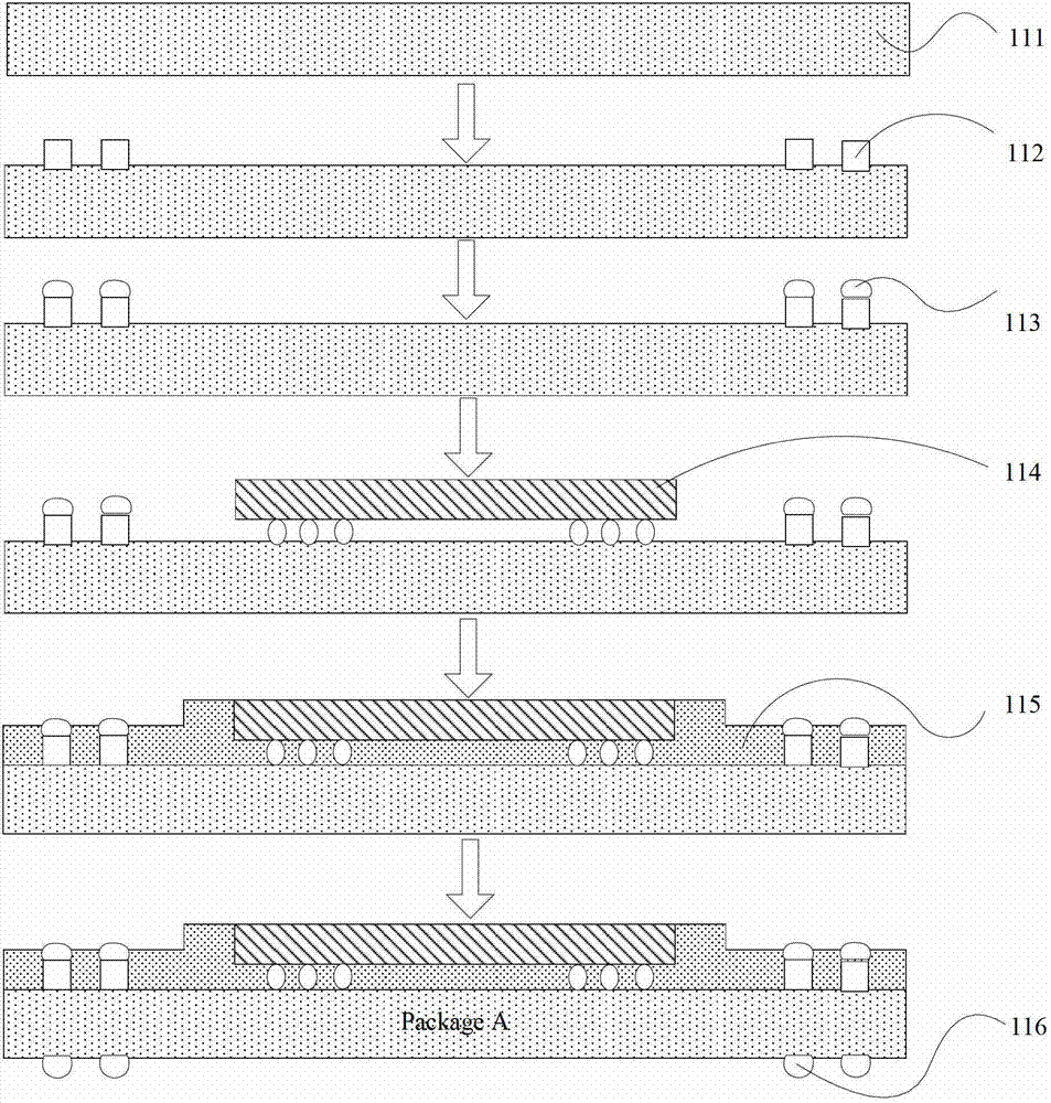
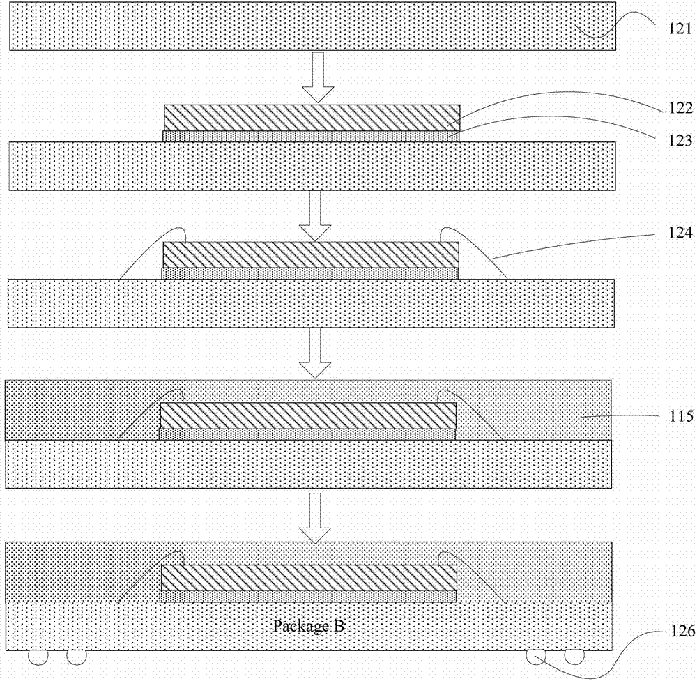
[0038] The present invention will be further described below in conjunction with specific drawings and embodiments.

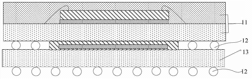
[0039] As mentioned in the background art, in the existing POP packaging technology, since the solder balls (ie, solder bumps) need to be higher than the height of the chip in the common process, it is impossible to achieve fine-pitch packaging interconnection. In the process of Shennan Company, although the copper pillars are made by electroplating and the balls are planted, relatively thin conductive vias can be produced, but the electroplating process itself is an expensive and cumbersome process, which affects the efficiency and efficiency of packaging. cost.

[0040] Therefore, the present invention proposes a new POP packaging structure and packaging method, which can achieve fine pitch between solder bumps by reducing the size of solder bumps themselves, which can help reduce the pitch size of solder bumps. In the prior art, soldering bumps are limited ...


PUM


Abstract

The invention provides a fine spacing laminated packaging structure containing a copper pillar, which comprises a lower packaging body and an upper packaging body, wherein the lower packaging body comprises a lower substrate, and a first chip is installed at a chip packaging area of the upper surface of the lower substrate and is electrically connected with the lower substrate; a welding area of the upper surface of the lower substrate is provided with the copper pillar, and a first welding ball is arranged on the copper pillar; the first welding ball and the upper surface of the lower substrate are pre-packaged by a packaging material, and the top of the first welding ball shows the packaging material of the upper surface of the lower substrate; the upper packaging body comprises an upper substrate, and a second chip is installed at the upper surface of the upper substrate and is electrically connected with the upper substrate; a welding area of the lower surface of the upper substrate is provided with a second welding ball. The upper substrate and the lower substrate are mutually connected through the butting joint of the second welding ball and the first welding ball. The packaging structure adopts the copper pillar so that the ball diameter of the welding balls can be shortened, and therefore the purpose of fine spacing packaging is achieved. As the copper pillar is manufactured in a welding line way, the complex electroplating process is omitted. The fine spacing laminated packaging structure has the advantages of simplicity in manufacture, low cost and the like.

Description

technical field [0001] The invention relates to the field of integrated circuit packaging, in particular to a fine-pitch stacked packaging structure and packaging method including copper pillars. Background technique [0002] With the continuous advancement of microelectronics technology, the feature size of integrated circuits has been continuously reduced and the interconnection density has been continuously increased. At the same time, users' requirements for high performance and low power consumption continue to increase. In this case, the way to improve the performance by further reducing the line width of the interconnection is limited by the physical characteristics of the material and the equipment process, and the resistance-capacitance (RC) delay of the two-dimensional interconnection gradually becomes the limit to improve the performance of the semiconductor chip. bottleneck. [0003] Chip stacking is one of the main ways to increase the density of electronic pa...

Claims


Application Information

Patent Timeline
Patent Type & Authority Applications(China)
IPC IPC(8): H01L23/538H01L21/768
CPCH01L2224/16225H01L2224/48091H01L2224/48227H01L2224/73265H01L2224/92247H01L2924/15311H01L2224/32225H01L24/16H01L24/45H01L24/48H01L24/73H01L24/92H01L25/105H01L2224/451H01L2224/73204H01L2224/73253H01L2224/92125H01L2924/15331H01L2924/1815H01L2924/18161H01L2924/19107H01L2224/0401H01L23/3128H01L2224/45147H01L2224/49H01L2924/181H01L2225/1023H01L2225/1058H01L2225/1076H01L24/81H01L24/85H01L2924/00014H01L2924/00012H01L2924/00H01L24/03H01L24/09H01L24/17H01L24/49H01L2224/04042H01L2224/11849H01L2224/13014H01L2224/16148H01L2224/1713H01L2224/48225H01L2224/81203H01L2224/81205H01L2224/85203H01L2224/85205H01L2924/01029H01L2924/01079
Inventor 陆建刚陆原黄卫东
Owner NAT CENT FOR ADVANCED PACKAGING CO LTD
Why Eureka
Try Eureka