

Method for forming film layer
A technology of film layer and gas, which is applied in the direction of coating, metal material coating process, gaseous chemical plating, etc.
- Summary
- Abstract
- Description
- Claims
- Application Information
AI Technical Summary
Problems solved by technology
Method used
Image

Examples
no. 1 example
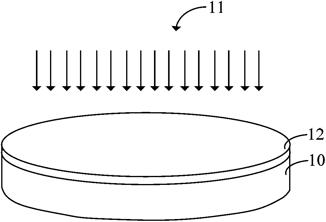
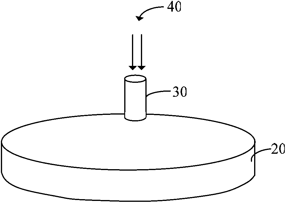
[0054] image 3 It is a schematic diagram of the three-dimensional structure of the method for forming a film layer according to the first embodiment of the present invention, Figure 4 It is a schematic cross-sectional structure diagram of the method for forming a film layer according to the first embodiment of the present invention, with reference to image 3 with Figure 4 , the method for forming a film layer according to the first embodiment of the present invention is specifically:
[0055] Step S21 is executed to provide a substrate 20 . The material of the substrate 20 can be single crystal silicon (Si), single crystal germanium (Ge), silicon germanium (GeSi), or silicon carbide (SiC); it can also be silicon on insulator (SOI) or germanium on insulator (GOI) ; or other materials, such as III-V group compounds such as gallium arsenide. A device structure is formed in the substrate 20, and the specific device structure is determined according to actual conditions.
...
no. 2 example
[0066] Image 6 It is a schematic diagram of the three-dimensional structure of the first pipe 30a in the second embodiment of the present invention, refer to Image 6 , In the second embodiment, the first tube 30a is a porous tube, including a plurality of tubes 31a and an outer tube 32a surrounding the tubes 31a, and there may or may not be a gap between the outer tube 32a and the tubes 31a. The shape of the outer tube 32a is the same as that of the first tube 30 in the first embodiment, and will not be repeated here. The shape of the pipe 31a is the same as that of the first pipe 30 in the first embodiment; the shape of the pipe 31a may be the same as or different from that of the outer pipe 32a.
[0067] In the second embodiment, the gases used to form the film layer are passed into the respective pipes 31a, one type of gas is passed into one pipe 31a, and the number of pipes 31a can be set according to the type of gas used to form the film layer. Of course, the type of ...
no. 3 example
[0070] Figure 7 It is a schematic diagram of the three-dimensional structure of the first tube and the second tube of the third embodiment of the present invention, refer to Figure 7 , compared with the first embodiment, in the third embodiment, the first tube 30 is covered with the second tube 50, and there is a gap 60 between the second tube 50 and the first tube 30; When the gas 40 for forming the film layer is passed into the gap 30, the cooling gas 70 is passed into the gap, so that the cooling gas reaches the periphery of the arrival position of the gas 40 for forming the film layer. The temperature of the cooling gas is lower than the gas used to form the film layer, and the specific temperature of the cooling gas can be limited according to actual requirements. The type of cooling gas 70 is not limited, as long as it does not affect the formation of the film layer. In this embodiment, since the cooling gas surrounds the gas used to form the film layer, the two are ...
PUM
| Property | Measurement | Unit |
|---|---|---|
| diameter | aaaaa | aaaaa |
Abstract
Description
Claims
Application Information