
The method of forming the film layer

A film and gas technology, used in coatings, metal material coating processes, gaseous chemical plating, etc.

Active Publication Date: 2015-09-02
SEMICON MFG INT (SHANGHAI) CORP
View PDF1 Cites 0 Cited by
  • Summary
  • Abstract
  • Description
  • Claims
  • Application Information

AI Technical Summary

Problems solved by technology

[0005] In the prior art, there are many methods for forming a film layer, such as the U.S. patent document US2012 / 0064717A1 published on March 15, 2012, however, none of which solves the above technical problems

Method used


Image

  • The method of forming the film layer
  • The method of forming the film layer
  • The method of forming the film layer

Examples


no. 1 example

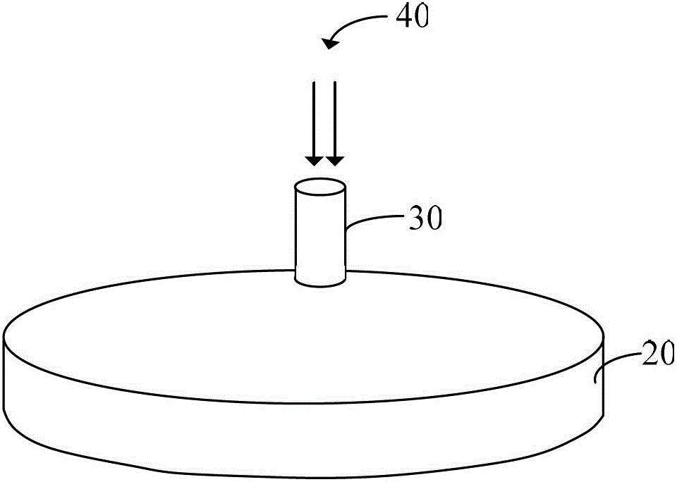
[0054] image 3 It is a schematic diagram of the three-dimensional structure of the method for forming a film layer according to the first embodiment of the present invention, Figure 4 It is a schematic cross-sectional structure diagram of the method for forming a film layer according to the first embodiment of the present invention, with reference to image 3 and Figure 4 , the method for forming a film layer according to the first embodiment of the present invention is specifically:

[0055] Step S21 is executed to provide a substrate 20 . The material of the substrate 20 can be single crystal silicon (Si), single crystal germanium (Ge), silicon germanium (GeSi), or silicon carbide (SiC); it can also be silicon on insulator (SOI) or germanium on insulator (GOI) ; or other materials, such as III-V group compounds such as gallium arsenide. A device structure is formed in the substrate 20, and the specific device structure is determined according to actual conditions.

...

no. 2 example

[0066] Figure 6 It is a schematic diagram of the three-dimensional structure of the first pipe 30a in the second embodiment of the present invention, refer to Figure 6 , In the second embodiment, the first tube 30a is a porous tube, including a plurality of tubes 31a and an outer tube 32a surrounding the tubes 31a, and there may or may not be a gap between the outer tube 32a and the tubes 31a. The shape of the outer tube 32a is the same as that of the first tube 30 in the first embodiment, and will not be repeated here. The shape of the pipe 31a is the same as that of the first pipe 30 in the first embodiment; the shape of the pipe 31a may be the same as or different from that of the outer pipe 32a.

[0067] In the second embodiment, the gases used to form the film layer are passed into the respective pipes 31a, one type of gas is passed into one pipe 31a, and the number of pipes 31a can be set according to the type of gas used to form the film layer. Of course, the type o...

no. 3 example

[0070] Figure 7 It is a schematic diagram of the three-dimensional structure of the first tube and the second tube of the third embodiment of the present invention, refer to Figure 7 , compared with the first embodiment, in the third embodiment, the first tube 30 is covered with the second tube 50, and there is a gap 60 between the second tube 50 and the first tube 30; When the gas 40 for forming the film layer is passed into the gap 30, the cooling gas 70 is passed into the gap, so that the cooling gas reaches the periphery of the arrival position of the gas 40 for forming the film layer. The temperature of the cooling gas is lower than the gas used to form the film layer, and the specific temperature of the cooling gas can be limited according to actual requirements. The type of cooling gas 70 is not limited, as long as it does not affect the formation of the film layer. In this embodiment, since the cooling gas surrounds the gas used to form the film layer, the two are ...


PUM

PropertyMeasurementUnit
diameteraaaaaaaaaa

Abstract

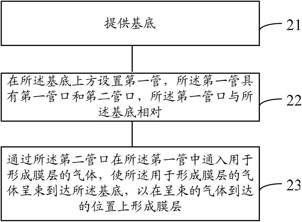
A method for forming a film layer comprises: a substrate is provided; a first tube is arranged above the substrate, the first tube has a first tube port and a second tube port, and the first tube port is opposite to the substrate; gas for forming the film layer is introduced into the first tube through the second tube port, so that the gas for forming the film layer is shaped as a beam to reach the substrate, and the film layer is formed at a position where the beam-shaped gas arrives. The technical scheme can realize a method for forming a high-temperature thin film in a low-temperature environment.

Description

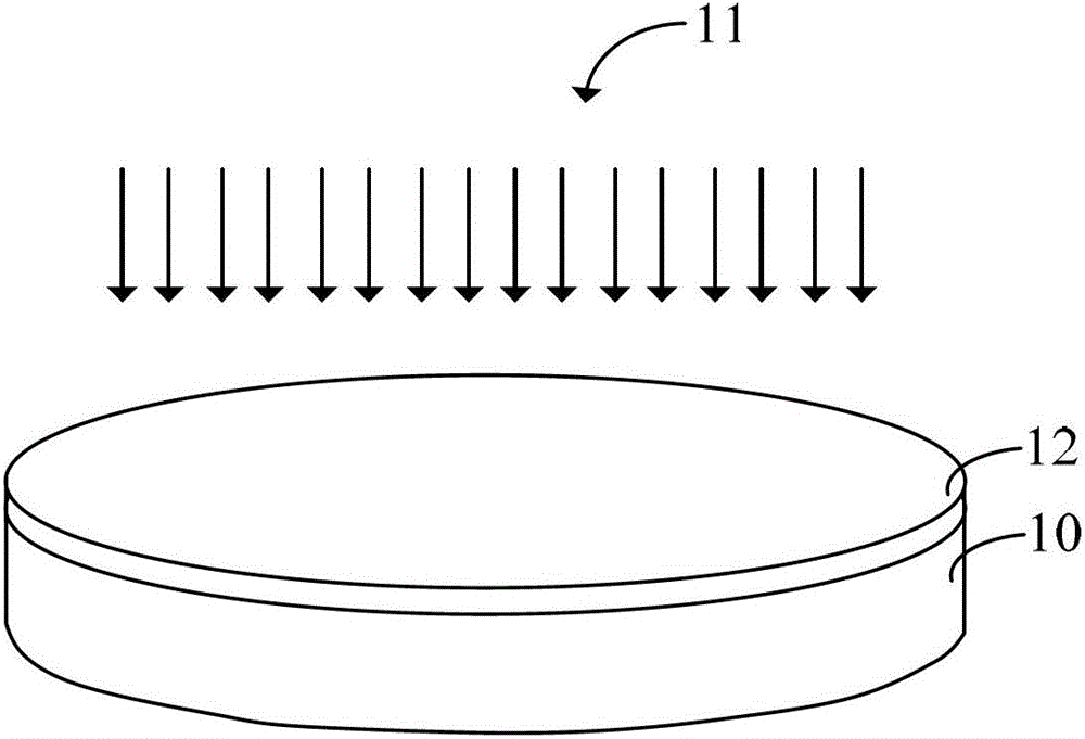
technical field [0001] The invention relates to the technical field of semiconductors, in particular to a method for forming a film layer. Background technique [0002] In the semiconductor process, the dielectric layer is usually formed by chemical vapor deposition (CVD, chemical vapor deposition), enhanced plasma chemical vapor deposition (PECVD, plasma enhanced chemical vapor deposition) or plasma chemical vapor deposition (PCVD, plasma chemical vapor deposition). , in CVD, PECVD and PCVD processes, the reaction gas or plasma on the wafer surface is a high-temperature gas or high-temperature plasma, usually the temperature can reach above 500 degrees Celsius. figure 1 It is a schematic diagram of a method for forming a film layer by enhanced plasma chemical vapor deposition in the prior art, refer to figure 1 , the method of forming a film layer includes: providing a substrate 10, on which other device structures (not shown in the figure) are formed; passing the enhanced...

Claims


Application Information

Patent Timeline
Patent Type & Authority Patents(China)
IPC IPC(8): C23C16/52C23C16/455
Inventor 王冬江张城龙张海洋
Owner SEMICON MFG INT (SHANGHAI) CORP
Learn More