Plasma etching device with even gas supply function and gas supply device thereof

A plasma and etching device technology, applied in electrical components, discharge tubes, circuits, etc., can solve the problems of uneven distribution of active particle density, affecting workpiece processing results, complex gas path structure, etc., to achieve simple structure and ensure uniformity. Sex, the effect of solving energy

Inactive Publication Date: 2013-12-04
CHINA UNIV OF GEOSCIENCES (BEIJING)
View PDF8 Cites 7 Cited by
  • Summary
  • Abstract
  • Description
  • Claims
  • Application Information

AI Technical Summary

Problems solved by technology

In order to ensure the uniformity of gas distribution in the reaction chamber as much as possible, there are usually many gas outlet holes on the gas distribution plate and the distribution range is large, which makes the corresponding gas path structure in the ground electrode connected with it on the gas path It becomes complicated, which leads to an increase in processing difficulty and an increase in cost
In addition, the air outlet holes on the gas distribution plate are usually evenly distributed, while the air inlet holes are usually located at the center of the upper end cover, and the directions of the air inlet holes and the air outlet holes are the same (both alon

Method used


Image

  • Plasma etching device with even gas supply function and gas supply device thereof
  • Plasma etching device with even gas supply function and gas supply device thereof
  • Plasma etching device with even gas supply function and gas supply device thereof

Examples


Embodiment Construction

[0037] Embodiments of the present invention will be described in detail below with reference to the drawings.

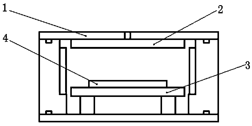
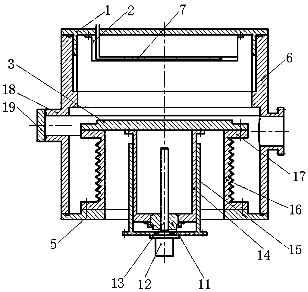
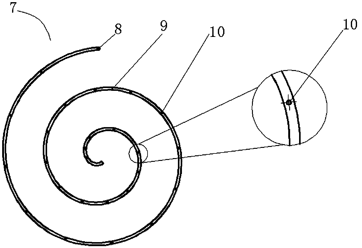
[0038] Such as figure 2As shown, the semiconductor etching device of the present invention includes a reaction chamber for performing plasma etching, the reaction chamber includes an upper end cover 1, a lower end cover 5, and a side wall 6, and the inside of the reaction chamber is provided with A ground electrode 2 and a radio frequency electrode 3, the ground electrode 2 is installed on the upper end cover 1 of the reaction chamber by screws, the stage carrying the semiconductor workpiece is arranged on the radio frequency electrode 3, and the inside of the reaction chamber is also provided with a A gas supply device 7 for supplying reaction gas to the semiconductor workpiece, and a workpiece pick-and-place device for picking and placing the semiconductor workpiece. The reaction gas and the auxiliary gas enter the reaction chamber through the gas supply device 7...


PUM


Abstract

Provided is a plasma etching device with the even gas supply function. The plasma etching device with the even gas supply function comprises a reaction chamber, wherein a grounding electrode and a radio-frequency electrode are arranged in the reaction chamber in an opposite and spaced mode. The plasma etching device with the even gas supply function further comprises a gas supply device. The gas supply device comprises at least one even gas pipeline, wherein a gas inlet is formed in one end of the even gas pipeline, the other end of the even gas pipeline is closed, a plurality of gas outlets are formed in the side wall of the even gas pipeline, the gas inlet of the even gas pipeline is formed outside the reaction chamber, and is inserted into the reaction chamber in a sealed mode, the portion, with the gas outlets, of the even gas pipeline, namely a gas exhaust pipe portion, is arranged between the grounding electrode and the radio-frequency electrode, and the gas outlets face a workpiece which is placed between the grounding electrode and the radio-frequency electrode. The invention further provides the gas supply device. According to the plasma etching device with the even gas supply function and the gas supply device, uniformity of distribution of gas pressure of gas inside the reaction chamber can be well improved through the reaction chamber, the rejection rate of workpieces can be reduced, and the service life of the reaction chamber can be prolonged.

Description

technical field [0001] The invention relates to a plasma etching device, in particular to a plasma etching device capable of uniform gas supply; the invention also provides a gas supply device for plasma etching. Background technique [0002] In the processing of VLSI, active particles (chloride ions, fluorine ions, etc.) in the plasma are usually used to etch, oxidize, PECVD (plasma-assisted chemical vapor deposition) and other treatments on semiconductors (single crystal silicon) craft. [0003] attached figure 1 It is a structural diagram of the reaction chamber of a plasma semiconductor etching device commonly used in the prior art, and the reaction gas and auxiliary gas enter the reaction chamber through the air inlet hole on the upper end cover 1 and the ground electrode 2 with a vent hole , RF bias is connected to the RF electrode 3, the gas is excited to form plasma in the space between the ground electrode 2 and the RF electrode 3, and bombards the semiconductor ...

Claims


Application Information

Patent Timeline
IPC IPC(8): H01J37/32
Inventor 杨义勇肖志杰刘伟峰程嘉季林红韩传锟赵康宁
Owner CHINA UNIV OF GEOSCIENCES (BEIJING)
Why Eureka
Try Eureka