Forming method of semiconductor device and forming method of fin type field effect transistor

一种鳍式场效应管、半导体的技术,应用在半导体器件、半导体/固态器件制造、电固体器件等方向,能够解决器件性能问题等问题,达到性能稳定、栅极漏电流小、沟道区载流子迁移率增加的效果

Active Publication Date: 2013-12-04
SEMICON MFG INT (SHANGHAI) CORP
View PDF2 Cites 9 Cited by
  • Summary
  • Abstract
  • Description
  • Claims
  • Application Information

AI Technical Summary

Problems solved by technology

[0004] However, as the process node is further reduced, there are problems with the device performance of the prior art FinFET

Method used


Image

  • Forming method of semiconductor device and forming method of fin type field effect transistor
  • Forming method of semiconductor device and forming method of fin type field effect transistor
  • Forming method of semiconductor device and forming method of fin type field effect transistor

Examples


Embodiment Construction

[0047] As mentioned in the background, the performance of the prior art FinFET is not stable.

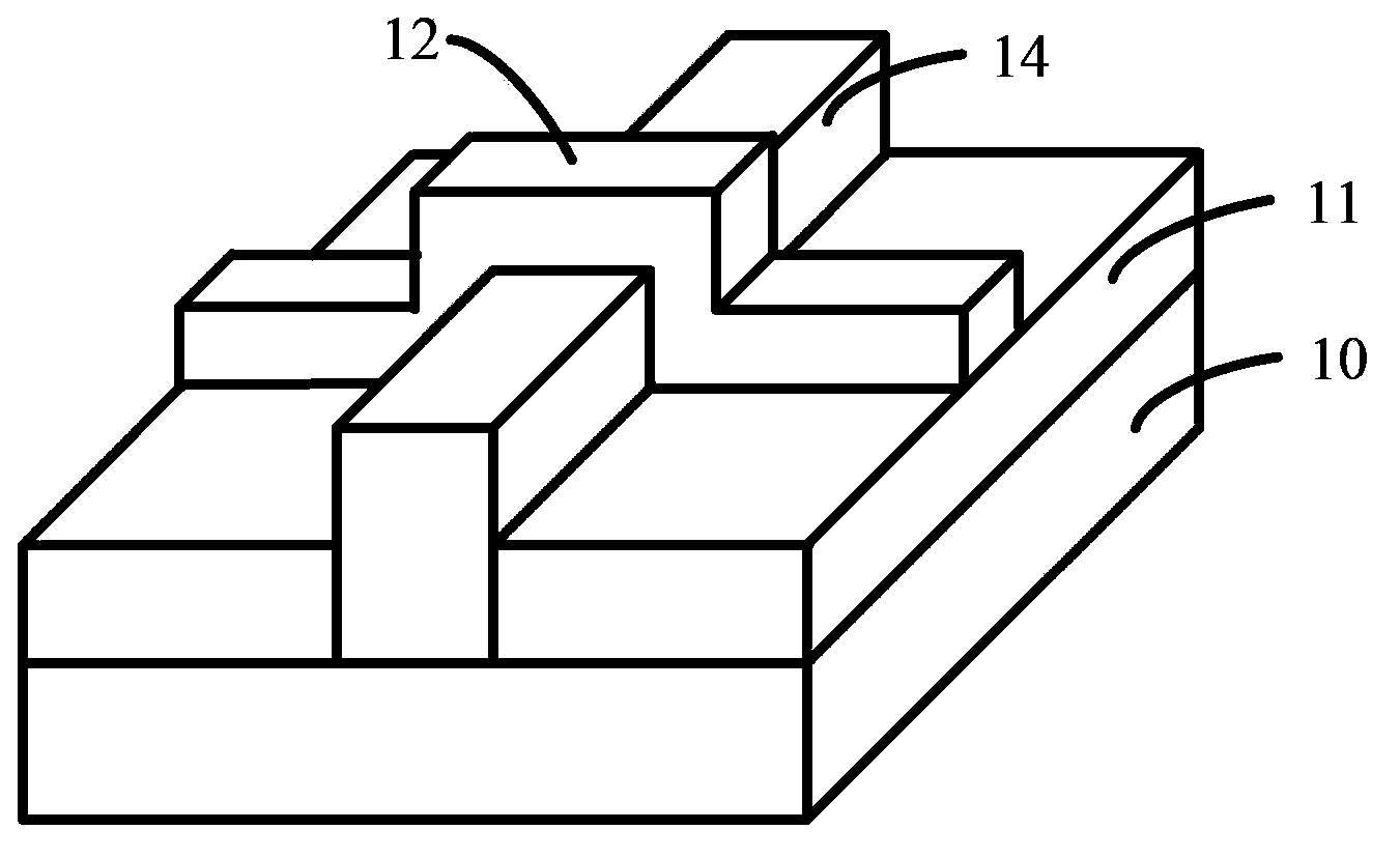
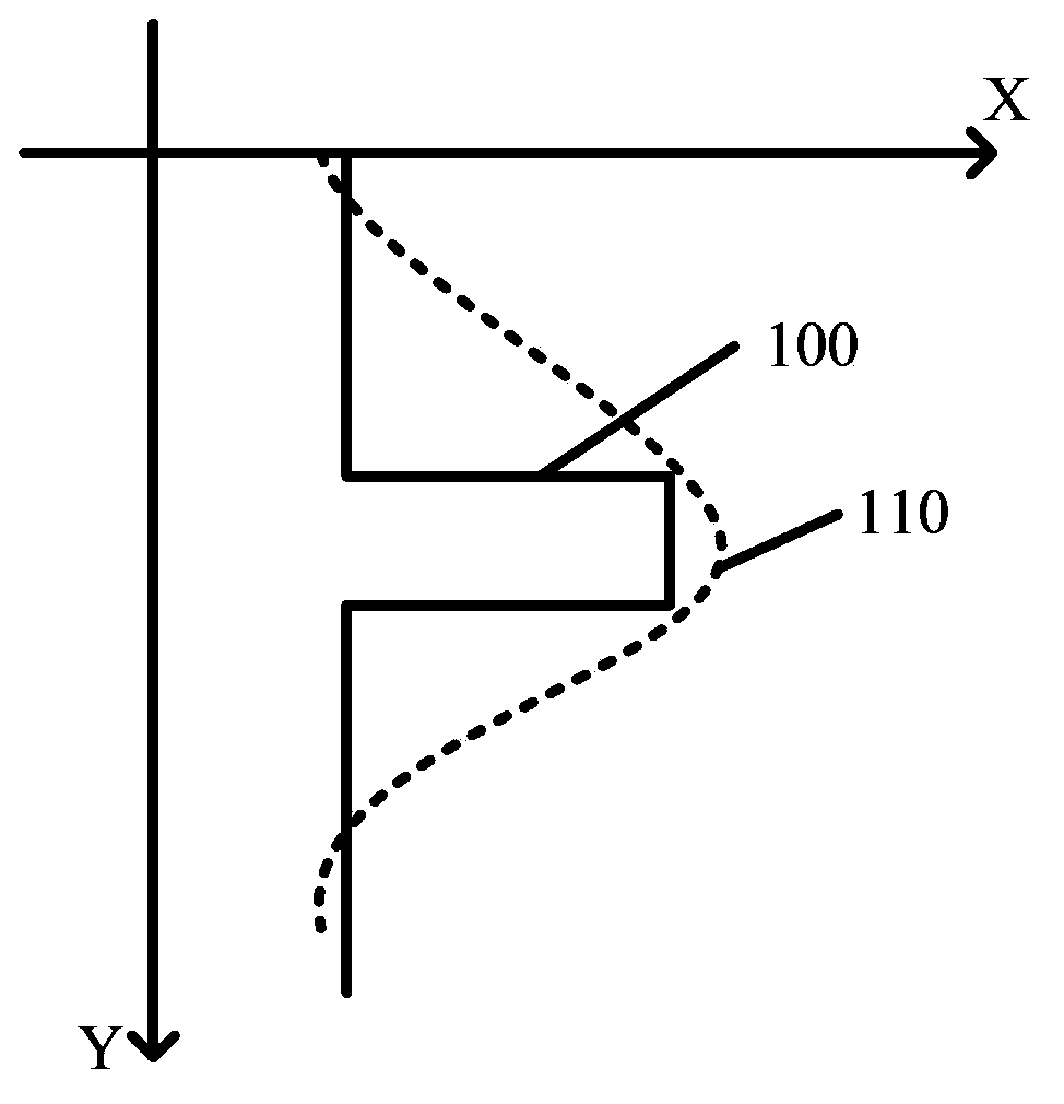
[0048] After research, the inventors found that there are many reasons affecting the performance stability of the fin field effect transistor, one of which is: the existing technology forms fins 14 on the surface of the semiconductor substrate (such as figure 1 As shown), when doping ions from the top surface of the fin 14 to the inside of the fin 14, as figure 2 as shown in figure 2 The middle X-axis represents the concentration of dopant ions in the fin 14, and the Y-axis represents the distance from any point in the fin 14 to the top of the fin 14. In the case of ideal doping, it is desired that the ion concentration after doping be within the fin 14 As shown in the curve 100, the dopant ions are concentrated in the middle of the fin 14, while the ion concentration at both ends of the fin 14 is less and evenly distributed; however, the actual doped ion concentration is in the ...


PUM

PropertyMeasurementUnit
temperatureaaaaaaaaaa

Abstract

The invention provides the forming method of a semiconductor device. The forming method comprises the steps of providing a semiconductor substrate; carrying out a doping process on the semiconductor substrate; forming a doped layer on the surface of the semiconductor substrate; forming a hard mask layer located on the surface of the doped layer; etching a part of the doped layer by using the hard mask layer as a mask; forming a first sub fin part; forming an insulating layer on the surface of the semiconductor substrate, wherein the surface of the insulating layer is flush with the top of the first sub fin part; after the insulating layer is formed, removing the first sub fin part of part of thickness to form an opening; and forming a second sub fin part within the opening, wherein the top of the second sub fin part is flush with the surface of the insulating layer. The invention further provides a forming method of a fin type field effect transistor. Formed semiconductor device and the fin type field effect transistor have the advantages of large channel region stress, high carrier mobility ratio, low threshold voltage, small gate leakage current and stable performance.

Description

technical field [0001] The invention relates to the technical field of semiconductor manufacturing, in particular to a method for forming a semiconductor device and a method for forming a fin field effect transistor. Background technique [0002] With the continuous development of semiconductor process technology, the process node is gradually reduced, and the gate-last (gate-last) process has been widely used to obtain an ideal threshold voltage and improve device performance. However, when the feature size (CD, Critical Dimension) of the device is further reduced, even if the gate-last process is adopted, the structure of the conventional MOS field effect transistor can no longer meet the requirements for device performance. Widespread concern. [0003] Fin field effect transistor (Fin FET) is a common multi-gate device, figure 1 A schematic diagram of a three-dimensional structure of a fin field effect transistor in the prior art is shown. Such as figure 1 As shown, i...

Claims


Application Information

Patent Timeline
Patent Type & Authority Applications(China)
IPC IPC(8): H01L21/336
CPCH01L21/845H01L27/0886H01L27/1211H01L29/66477H01L21/823431H01L29/785H01L21/823821H01L27/0924H01L29/1054
Inventor 三重野文健
Owner SEMICON MFG INT (SHANGHAI) CORP
Why Eureka
Try Eureka