Smart card carrier tape manufacturing method

A manufacturing method and technology for smart cards, which are applied in the manufacture of semiconductor/solid-state devices, electrical components, circuits, etc., can solve the problems of polluting the environment and large consumption of materials, protect the environment, overcome the huge consumption of materials, reduce the consumption of metal materials and The effect of processing costs

Inactive Publication Date: 2013-12-04
SHANGHAI YIDIAN ELECTRONICS PRINTING TECH +1
View PDF5 Cites 7 Cited by
  • Summary
  • Abstract
  • Description
  • Claims
  • Application Information

AI Technical Summary

Problems solved by technology

[0009] In view of the above-mentioned problems, the present invention provides a method for manufacturing a smart card carrier tape, to overcome the problem of huge material consumption due to the use of the etching process in the prior art, and also to overcome the large amount of waste caused by the use of the etching process in the prior art. waste water, which seriously pollutes the environment, thus reducing the production cost of the carrier tape

Method used


Image

  • Smart card carrier tape manufacturing method
  • Smart card carrier tape manufacturing method
  • Smart card carrier tape manufacturing method

Examples


Embodiment 1

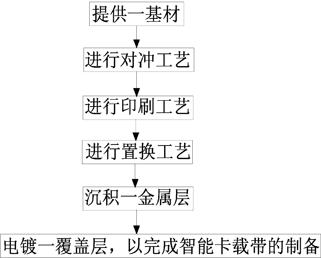
[0043] figure 1 It is a schematic flow chart of the manufacturing method of the smart card carrier tape provided by the embodiment 1 of the present invention; mixture, and the thickness of the substrate is 0.05mm-0.125mm, such as 0.05mm, 0.08mm, 0.10mm, 0.11mm, 0.12mm, 0.125mm, etc.

[0044] The base material provided above is subjected to a hedging process by means of mechanical drilling or laser drilling, so as to form alignment holes required by the process on the base material.

[0045]Then, the printing process is carried out on the substrate with the alignment holes formed. The printing process includes: printing the catalytic ink onto the above-mentioned alignment holes by using screen printing method, flexographic printing method, letterpress printing method or gravure printing method. On the base material, use hot air curing method or infrared curing method, and perform curing operation at a temperature of 130°C to 150°C, such as 130°C, 135°C, 140°C, 145°C, 150°C, et...

Embodiment 2

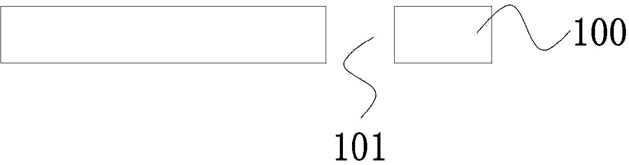
[0053] figure 2 It is a schematic diagram of the structure of the alignment hole formed on the substrate provided by Example 2 of the present invention; The required alignment hole 101.

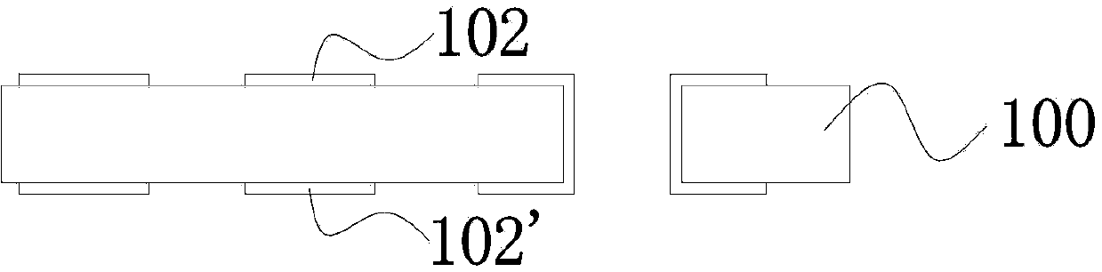
[0054] image 3 It is a schematic diagram of the structure of the metal seed layer provided by Example 2 of the present invention; as shown in the figure, the printing process is performed on both the front and back sides of the substrate 100 that has formed the alignment hole 101. The printing process includes: using screen printing Method, flexographic printing method, letterpress printing method or gravure printing method, the catalytic ink is printed on the front and back surfaces of the substrate 100 with the above-mentioned alignment holes 101 formed, and then hot air curing method or infrared curing method is used. 130°C ~ 150°C, such as 130°C, 135°C, 140°C, 145°C, 150°C, etc., for curing operation, and the time for curing operation is 40min ~ 60min, such as 40min, 42min, 48min, 52m...


PUM


Abstract

The invention discloses a smart card carrier tape manufacturing method including forming a catalytic ink graphic layer on a substrate by printing the catalytic ink onto the substrate, forming a metal seeding layer by means of replacement, and performing metal planting and coating planting processes to complete the manufacturing of the smart card carrier tapes. In the smart card carrier tape manufacturing method, manufacturing processes of the smart card carrier tapes in the prior art are simplified and consumption of metal materials and processing cost are reduced; since the etching process is removed, the problem of high material consumption caused by the etching process in the prior art is solved, severe environment pollution caused by a great quantity of waste water generated during the etching process in the prior art is overcome, production cost is reduced while competitive rate of products is increased, the purposes of saving work and materials are achieved while waste water and pollutant are reduced, and accordingly environments are protected while green production is realized.

Description

technical field [0001] The invention relates to a manufacturing method, in particular to a manufacturing method of a smart card carrier tape. Background technique [0002] In today's information age, smart cards can be seen everywhere in our daily life. In the term used by the International Organization for Standardization, smart cards are ICC, that is: integrated circuit cards. With the development of smart card technology, smart cards have been widely used in mobile communications and public telephones, traffic management, social insurance, population management, internal management of enterprises and institutions, taxation, petroleum, public utility charges, etc. In addition, with the comprehensive promotion of financial cards, the application of smart cards in the financial field is gradually increasing. [0003] In the global smart card market in 2010, the Asia-Pacific region accounted for about 71.5% of the market share, of which the Chinese market accounted for one-t...

Claims


Application Information

Patent Timeline
Patent Type & Authority Applications(China)
IPC IPC(8): H01L21/48
Inventor 马克庄红曹晶强勇潘靖雷
Owner SHANGHAI YIDIAN ELECTRONICS PRINTING TECH
Why Eureka
Try Eureka