

Multilayer hexagonal substrate integrated waveguide filter
A substrate-integrated waveguide and hexagonal technology, applied in waveguide devices, electrical components, circuits, etc., can solve the problems of increased design difficulty, increased filter volume, and higher loss
- Summary
- Abstract
- Description
- Claims
- Application Information
AI Technical Summary
Problems solved by technology
Method used
Image

Examples
Embodiment
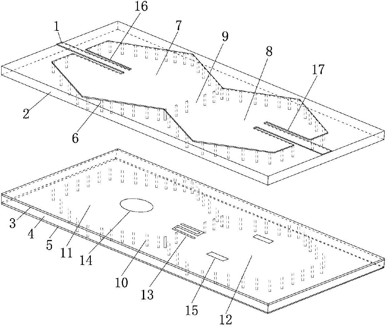
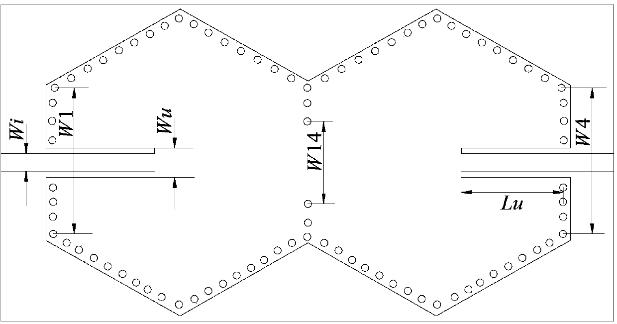
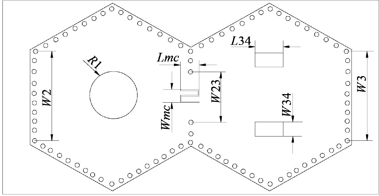
[0021] In this embodiment, the material of the first dielectric substrate 2 and the second dielectric substrate 4 of the multilayer hexagonal substrate integrated waveguide filter is a Ferro-A6M ceramic substrate, and the relative permittivity ε r =5.9, the loss tangent is 0.0015, and the single layer thickness after sintering is 0.096mm. Each layer of dielectric substrate is composed of four layers of ceramic substrates. The first metal layer 1, the second metal layer 3, and the third metal layer 5 are made of gold or silver, with a thickness of 8-12um, and the through hole filling material is gold or silver. , The diameter of the through hole is 0.17~0.22mm, and the hole spacing is 0.45~0.65mm. The specific structural dimensions of the multilayer hexagonal substrate integrated waveguide filter are marked as figure 2 , image 3 As shown, the specific corresponding parameters are shown in the following table:
[0022] parameters
[0023] The transmission characte...
PUM
 Abstract
Description
Claims
Application Information