
Optical Parametric Oscillator Laser Based on Wide Bandgap Semiconductor Silicon Carbide Crystal

A wide bandgap semiconductor, optical parametric oscillation technology, applied in the direction of active medium materials, etc., can solve the problems of unreported OPO lasers, SiC crystal materials have not been paid attention to, and achieve high cost performance, low cost, and easy installation and adjustment. Effect

Active Publication Date: 2015-12-23
SHANDONG UNIV
View PDF6 Cites 0 Cited by
  • Summary
  • Abstract
  • Description
  • Claims
  • Application Information

AI Technical Summary

Problems solved by technology

However, the application of SiC crystal materials in the field of OPO has not been paid attention to, and OPO lasers based on wide-bandgap semiconductor SiC crystals have not been reported so far.

Method used


Image

  • Optical Parametric Oscillator Laser Based on Wide Bandgap Semiconductor Silicon Carbide Crystal

Examples


Embodiment 1

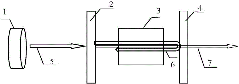
[0031] Optical parametric oscillator laser structure such as figure 1 As shown, it is composed of an excitation source 1, an input mirror 2, a semiconductor SiC crystal 3, and an output mirror 4, wherein: the excitation source 1 is Nd:YAG (neodymium-doped yttrium aluminum garnet, Nd-doped The impurity concentration is 1at.%) Q-switched laser; the input mirror 2 is a plane mirror, and its transparent surface is coated with a dielectric film with high transmission to 1.06 μm and high reflection to 1.57 μm and 3.26 μm; semiconductor SiC crystal 3 is 4H Type SiC single crystal, the angle between the direction of light transmission and the optical axis is 54.2°, the crystal length in the direction of light transmission is 30mm, the light transmission surface is polished and plated with high transmission dielectric film for 1.06μm, 1.57μm and 3.26μm; the output mirror 4 is a flat mirror , its two clear surfaces are coated with a dielectric film with a high reflection of 1.57μm and a...

Embodiment 2

[0033] As described in Example 1, the difference is that the two transparent surfaces of the output mirror 4 are coated with a dielectric film with a high reflection of 3.26 μm and a partial transmission of 1.57 μm (the transmittance is 50%), the output mirror and the output mirror The distance between them is 80mm. Increasing the excitation power can achieve 1.57μm mid-infrared OPO laser output.

Embodiment 3

[0035] As described in Example 1, the difference is that the output mirror 4 is a concave mirror with a radius of curvature of 50 mm, and the distance between the output mirrors is 80 mm. Increase the excitation power to obtain a 3.26 μm mid-infrared OPO laser output.


PUM


Abstract

The invention relates to an optical parametric oscillation laser based on wide-band-gap semiconductor silicon carbide crystals. The optical parametric oscillation laser sequentially comprises an excitation source, an input mirror, the semiconductor SiC crystals and an output mirror. The semiconductor SiC crystals are cut in the phase position matching direction of optical parametric oscillation of the semiconductor SiC crystals, medium membranes which allow much excitation light, much signal frequency light and much idler frequency light to penetrate through are plated on light-permeable faces respectively, the excitation source is an all-solid-state pulsed laser, medium membranes which allow much excitation light to penetrate through and allow much frequency light and much idler frequency light to be reflected are plated on the two light-permeable faces of the input mirror respectively, and a medium membrane which allows much frequency light to be reflected and allows idler frequency light to partially penetrate through is plated on the input mirror. The wide-band-gap semiconductor silicon carbide crystals are used as a non-linear optical medium, therefore, the optical parametric oscillation laser ranging from 1.28 micrometers to 6 micrometers are output, the output energy is high, the structure is simple, and the penetrating range is continuous and adjustable.

Description

technical field [0001] The invention relates to an optical parametric oscillation laser based on a wide bandgap semiconductor silicon carbide crystal (SiC), belongs to the field of laser technology, and relates to a nonlinear crystal device. Background technique [0002] Optical parametric oscillation refers to when a strong laser with a frequency of vP (pump frequency, also called excitation light) and a weak laser with a frequency of vS (signal frequency) are injected into a nonlinear medium at the same time, such as signal frequency light (also called Oscillating light) is amplified, and at the same time generate idle frequency light with frequency vi (idle frequency light, vi=vP-vS), which is the OPO laser to be obtained. This phenomenon is called optical parametric amplification. If this nonlinear medium is placed in the resonant cavity composed of the input mirror M1 and the output mirror M2, M1 transmits the pump frequency light, and M1 and M2 highly reflect the signa...

Claims


Application Information

Patent Timeline
Patent Type & Authority Patents(China)
IPC IPC(8): H01S3/16
Inventor 于浩海徐现刚路大治陈秀芳胡小波张怀金
Owner SHANDONG UNIV
Learn More