Stress-reducing laser chip structure and heat sink structure and preparation method thereof

A chip structure and laser technology, applied in the direction of lasers, laser parts, semiconductor lasers, etc., can solve the problem of not being able to fully meet the requirements of high-power semiconductor lasers, limiting the application of high-power semiconductor laser bars, and large stress of semiconductor laser bars, etc. problem, to achieve the effect of low bending, stress reduction and production cost reduction

Active Publication Date: 2016-06-08
WUHU ANRUI LASER TECH CO LTD
View PDF5 Cites 1 Cited by
  • Summary
  • Abstract
  • Description
  • Claims
  • Application Information

AI Technical Summary

Problems solved by technology

The stress of semiconductor laser bars packaged with this heat sink structure is relatively large, and the chip is prone to bending, which seriously limits the application of high-power semiconductor laser bars in fiber coupling and optical shaping.
[0006] In summary, the current packaging heat sink structure cannot fully meet the requirements of high-power semiconductor lasers

Method used


Image

  • Stress-reducing laser chip structure and heat sink structure and preparation method thereof
  • Stress-reducing laser chip structure and heat sink structure and preparation method thereof
  • Stress-reducing laser chip structure and heat sink structure and preparation method thereof

Examples


Embodiment 1

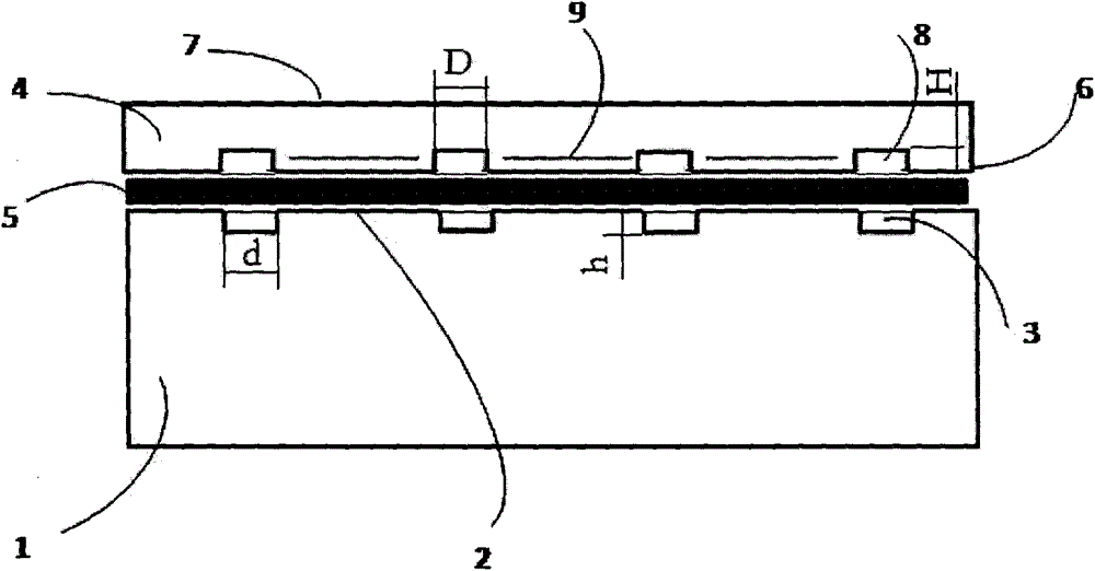
[0046] like figure 1 As shown, a stress-reducing laser chip structure includes a laser chip main body 4, the laser chip main body 4 has a positive electrode 6 and a negative electrode 7 electrically connected to an external electrode, a plurality of light emitting parts 9 are arranged on the positive electrode 6, and the light emitting parts 9 is provided with a first groove 8, and also includes a heat sink structure, the heat sink structure includes a heat sink body 1, the front side 2 of the heat sink body 1 is welded on the positive electrode 6 of the laser chip body 4 through a solder layer 5, and the heat sink structure includes a heat sink body 1. A second groove 3 is formed on the part of the sinker body 1 corresponding to the first groove 8 of the laser chip body 4 , and the second groove 3 corresponds to the first groove 8 one by one.

[0047]The heat sink body 1 is made of metal or ceramic or diamond or metal matrix composite. The metal matrix composite material can...

Embodiment 2

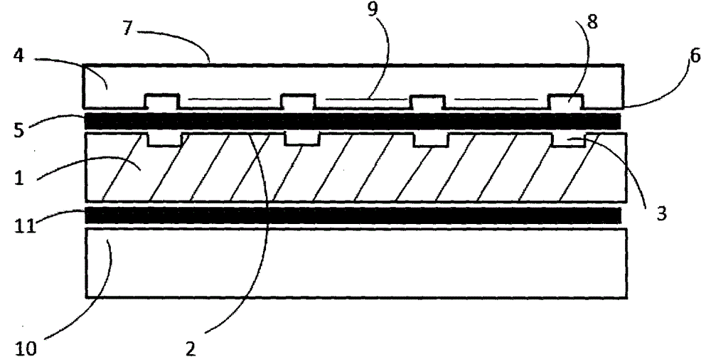
[0065] like figure 2 As shown, a stress-reducing laser chip structure includes a laser chip main body 4, the laser chip main body 4 has a positive electrode 6 and a negative electrode 7 electrically connected to an external electrode, a plurality of light emitting parts 9 are arranged on the positive electrode 6, and the light emitting parts 9 is provided with a first groove 8, and also includes a heat sink structure, the heat sink structure includes a heat sink body 1, the front side 2 of the heat sink body 1 is welded on the positive electrode 6 of the laser chip body 4 through a solder layer 5, and the heat sink structure includes a heat sink body 1. A second groove 3 is formed on the part of the sinker body 1 corresponding to the first groove 8 of the laser chip body 4 , and the second groove 3 corresponds to the first groove 8 one by one. The heat sink structure further includes a metal structure layer 10 , and the back surface of the heat sink body 1 is plated on the me...


PUM


Abstract

A stress-reducing laser chip structure comprises a laser chip body (4), the laser chip body (4) is provided with a positive pole (6) and a negative pole (7) that is electrically connected to an external electrode, a plurality of light-emitting portions (9) is disposed on the positive pole (6), and a first groove (8) is disposed between the light-emitting portions (9). The laser chip structure further comprises a heat sink structure, the heat sink structure comprises a heat sink body (1), a front surface (2) of the heat sink body (1) is welded to the positive pole (6) of the laser chip body (4) by using a solder layer (5), a portion, corresponding to the first groove (8) of the laser chip body (4), of the heat sink body (1) is provided with a second groove (3), and the second groove (3) corresponds to the first groove (8) one by one. The laser chip structure has a low stress state and a low curvature, can implement low-stress or "stress-free" packaging without affecting a thermal conduction capability of a laser, and can ensure long-time working of the laser.

Description

technical field [0001] The invention relates to a stress-reducing laser chip structure, a heat sink structure and a preparation method thereof, belonging to the field of laser manufacturing. Background technique [0002] At present, semiconductor lasers are also called laser diodes (LaserDiode). With the development and progress of semiconductor laser technology, its output power, electro-optical conversion efficiency, reliability and life are constantly improving, and it can be widely used in laser pumping, laser processing, laser ranging, scientific research and medical treatment, etc. The market demand is huge . [0003] Although semiconductor laser technology has made rapid progress, with the development of various application fields, higher requirements are placed on the performance of semiconductor lasers. High-quality fiber coupling and optical shaping products require semiconductor laser chips to have low chip curvature, that is, a small "smile" effect, high reliab...

Claims


Application Information

Patent Timeline
Patent Type & Authority Patents(China)
IPC IPC(8): H01S5/022H01S5/024
CPCH01S5/02476H01S5/02484H01S5/4031H01S5/0237
Inventor 李丰
Owner WUHU ANRUI LASER TECH CO LTD
Why Eureka
Try Eureka