Back side illumination image sensor and method for reducing dark current of back side illumination image sensor

An image sensor, back-illuminated technology, applied in circuits, electrical components, electrical solid devices, etc., can solve problems such as large dark current, and achieve the effect of preventing dark current

Active Publication Date: 2013-12-11
GALAXYCORE SHANGHAI
View PDF8 Cites 14 Cited by
  • Summary
  • Abstract
  • Description
  • Claims
  • Application Information

AI Technical Summary

Problems solved by technology

[0007] The problem solved by the present invention is to provide a back-illuminated image sensor and a method for reducing the dark curren...

Method used


Image

  • Back side illumination image sensor and method for reducing dark current of back side illumination image sensor
  • Back side illumination image sensor and method for reducing dark current of back side illumination image sensor

Examples


Embodiment Construction

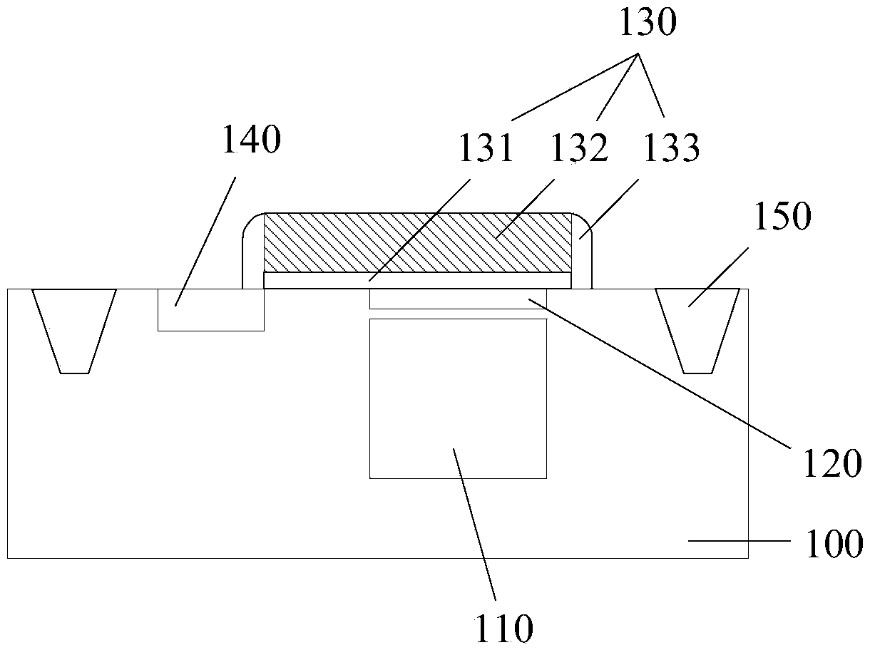
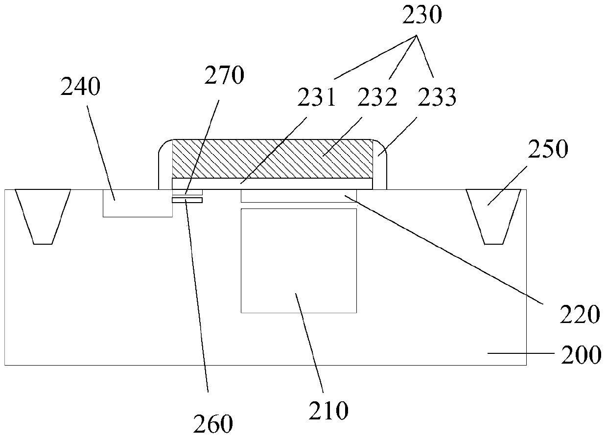
[0033] A back-illuminated image sensor generally includes a photodiode for receiving light to generate photocharges and a transfer transistor for transferring the photocharges to a floating diffusion region (Floating Diffusion, FD). In the back-illuminated image sensor, when forming the gate of the transfer transistor and the corresponding gate spacer, various etching processes will be performed, and the etching process will also affect the surface of the substrate directly above the photodiode. Etching will cause more defects on the surface of part of the substrate, and these defects will cause the semiconductor substrate material on the surface to generate deep energy levels, thereby causing the semiconductor substrate material to easily generate carriers even in the absence of light. These carriers are easily transferred into the photodiode under the defect, leading to the generation of dark current.

[0034] To this end, the present invention provides a back-illuminated im...


PUM


Abstract

The invention discloses a back side illumination image sensor and a method for reducing the dark current of the back side illumination image sensor. The back side illumination image sensor comprises a photodiode, a first conductive type isolated layer, a gate structure of a pass transistor, and a floating diffusion zone, wherein the gate structure corresponds to the first conductive type isolated layer and is formed on the upper surface of a first conductive type semiconductor substrate, the gate structure comprises a gate oxide, a grid layer and a grid side wall, the gate structure correspondingly covers the photodiode, and the floating diffusion zone is formed in the first conductive type semiconductor substrate and is provided with second conductive type heavy doping. In the back side illumination image sensor, the defects do not easily appear at the portion, over the photodiode, of the surface of the first conductive type semiconductor substrate, and therefore the dark current is effectively prevented from being produced.

Description

technical field [0001] The invention relates to the technical field of semiconductors, in particular to a back-illuminated image sensor and a method for reducing dark current of the back-illuminated image sensor. Background technique [0002] Image sensors are semiconductor devices that convert optical signals into electrical signals. The image sensor includes a photodiode (photo diode, PD) for sensing light and a logic circuit for converting the sensed light into an electrical signal. [0003] Conventional image sensors have a front-side illuminated structure in which photodiodes are formed below the substrate surface, logic circuits are formed above the photodiodes, and light reaches the photodiodes after passing through the logic circuits, during which light passes through the multilayer structure, resulting in Light loss or crosstalk of light to adjacent image sensor unit chips affects the photoresponse characteristics of the photodiodes of each image sensor unit chip. ...

Claims


Application Information

Patent Timeline
IPC IPC(8): H01L27/146
CPCH01L27/1464H01L27/14612H01L27/14616H01L27/1463
Inventor 李文强赵立新李杰徐泽
Owner GALAXYCORE SHANGHAI
Why Eureka
Try Eureka