LED (Light Emitting Diode) chip manufacturing technology, LED chip structure and LED chip packaging structure

A LED chip and manufacturing process technology, which is applied in the direction of electrical components, electrical solid devices, circuits, etc., can solve the problems of large difference in expansion coefficient of GaN silicon, high cost, and easy cracking, so as to optimize the packaging structure design and prevent deformation. Yellow, high reliability effect

Active Publication Date: 2013-12-11
江西量一光电科技有限公司
View PDF3 Cites 7 Cited by
  • Summary
  • Abstract
  • Description
  • Claims
  • Application Information

AI Technical Summary

Problems solved by technology

After using silicon carbide as the substrate, it can indeed greatly improve its heat dissipation, but its cost is too high. Recently, domestic manufacturers have begun to use silicon materials as the substrate, and the performance is better than that of sapphire. The only problem is that the expansion coefficient of GaN is too different from that of silicon. large and prone to cracking

Method used


Image

  • LED (Light Emitting Diode) chip manufacturing technology, LED chip structure and LED chip packaging structure
  • LED (Light Emitting Diode) chip manufacturing technology, LED chip structure and LED chip packaging structure
  • LED (Light Emitting Diode) chip manufacturing technology, LED chip structure and LED chip packaging structure

Examples


Embodiment Construction

[0021] The present invention will be further described below in conjunction with specific embodiments and accompanying drawings.

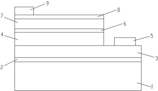
[0022] In the manufacturing process of the LED chip of the present invention, tungsten-molybdenum-copper alloy (WMoCu) is used as the substrate instead of commonly used sapphire and silicon carbide materials as the substrate. The weight percentage of tungsten in the tungsten-molybdenum-copper alloy is 84%-90%, and the balance is molybdenum and copper.

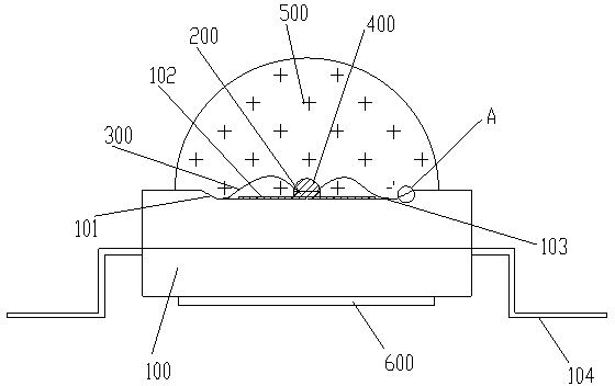
[0023] The manufacturing process is specifically: using tungsten-molybdenum-copper alloy as the substrate layer, epitaxially growing an AlN buffer layer on the tungsten-molybdenum-copper substrate layer, and then growing an n-type GaN layer, an InGaN / GaN multi-quantum well light-emitting layer, a p-type AlGaN layer, The p-type GaN layer, and then sequentially fabricate the current spreading layer and the P electrode on the surface of the p-type GaN layer; then transfer the epitaxial layer to the con...


PUM

PropertyMeasurementUnit
electrical resistivityaaaaaaaaaa
thicknessaaaaaaaaaa

Abstract

The invention relates to an LED (Light Emitting Diode) chip manufacturing technology, an LED chip structure and an LED chip packaging structure. According to the manufacturing technology, wolfram-molybdenum-copper alloy (WMoCu) is used as a substrate. The wolfram-molybdenum-copper alloy substrate is a good choice for a high-power LED chip heat dissipation substrate as the wolfram-molybdenum-copper alloy substrate has the thermal conductivity second only to that of a silicon carbide substrate, the cost of the wolfram-molybdenum-copper alloy substrate is far lower than that of the silicon carbide substrate, and meanwhile the wolfram-molybdenum-copper alloy substrate has the advantages of high temperature resistance, low expansion factor, high specific heat capacity, good mechanical machining property, easiness in manufacturing of mirror surfaces and the like. An LED chip in the invention sequentially comprises a wolfram-molybdenum-copper substrate layer, a U-GaN buffer layer and a N-type GaN layer from bottom to top, wherein an InGaN / GaN multiple-quantum well luminous layer and an N-electrode are arranged on the surface of the N-type GaN layer, and a P-type AlGaN layer, a P-type GaN layer, a current expanding layer and a P-electrode are also sequentially arranged above the InGaN / GaN multiple-quantum well luminous layer. Correspondingly, the LED chip has the advantages that the currents of the LED chip are vertically distributed, the substrate has high thermal conductivity and high reliability, the back surface of the luminous layer is a metal reflecting mirror, the surface has a coarsening structure, and the extraction efficiency is high.

Description

technical field [0001] The invention belongs to the field of LED technology, and in particular refers to a manufacturing process of an LED chip, an LED chip structure and an LED packaging structure. Background technique [0002] In the manufacture of LED chips, there are some problems in using sapphire as a substrate, such as lattice mismatch and thermal stress mismatch, which will cause a large number of defects in the epitaxial layer, and at the same time cause difficulties for the subsequent device processing technology. Sapphire is an insulator with a resistivity greater than 1011Ω·cm at room temperature. In this case, it is impossible to make a vertical structure device; usually only n-type and p-type electrodes are made on the upper surface of the epitaxial layer. Fabricating two electrodes on the upper surface reduces the effective light-emitting area and increases the photolithography and etching process in device manufacturing, resulting in reduced material utilizat...

Claims


Application Information

Patent Timeline
Patent Type & Authority Applications(China)
IPC IPC(8): H01L33/64H01L33/00H01L33/56H01L33/60H01L33/48H01L33/62
CPCH01L2224/48091H01L2224/8592H01L2924/181H01L2924/00014H01L2924/00012
Inventor 廖昆
Owner 江西量一光电科技有限公司
Why Eureka
Try Eureka