
Method for realizing welding between soft base chip circuit board and metal base body without special tool

A metal substrate and welding method technology, which is applied in the field of welding soft substrate circuit boards and metal substrates without special tooling, can solve problems such as increased production costs, difficult production site management, and unstable products, and reduce production costs. , Eliminate the design of special tooling and outsourcing processing processes, and ensure the effect of consistency

Active Publication Date: 2013-12-18
10TH RES INST OF CETC
View PDF4 Cites 10 Cited by
  • Summary
  • Abstract
  • Description
  • Claims
  • Application Information

AI Technical Summary

Problems solved by technology

[0006] In terms of management and cost: The products in the trial production, pre-research, and development stages are unstable, and there are links to repeatedly adjust the circuit and structure. Every time the adjustment is made, the tooling plate needs to be redesigned and processed, and the original tooling fixtures are idle or scrapped. , and there may be multiple batches of special tooling for the same project, making it difficult to manage the production site, and the production cost will also increase accordingly

Method used


Image

  • Method for realizing welding between soft base chip circuit board and metal base body without special tool
  • Method for realizing welding between soft base chip circuit board and metal base body without special tool

Examples


Embodiment Construction

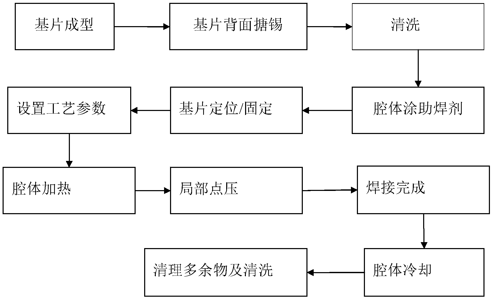
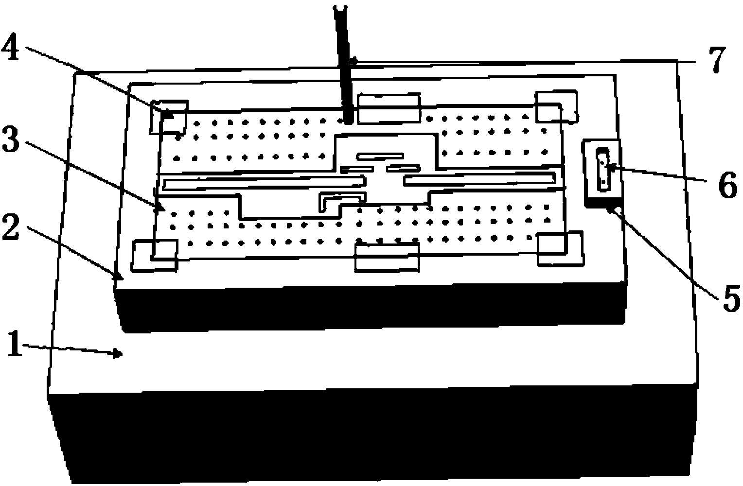
[0019] refer to figure 1 , figure 2 . The present invention will be described step by step below in conjunction with the accompanying drawings and examples.

[0020] The design of the exhaust hole on the soft substrate circuit board: metallization of φ0.3mm~φ0.8mm is set in the metal grounding area of ​​the soft substrate circuit board 3, and the hole density is 0.6cm 2 Inside, 3 to 4 exhaust through holes are evenly distributed in any 10mm diameter surface, and the hole spacing can be in accordance with the general design control requirements. As many ground holes as possible should be designed in the center and around the soft substrate printed circuit board 3 .

[0021] Tinning on the back of the soft substrate circuit board 3: the soft substrate circuit board 3 obtained by forming the circuit pattern is more or less warped or uneven in shape, and tinned on the back of the soft substrate circuit board 3 , the hardness of the circuit of the soft substrate circuit board 3...


PUM


Abstract

The invention provides a method for realizing welding between a soft base chip circuit board and a metal base body without a special tool, and aims to provide a local point-pressing welding method for the soft base chip circuit, which is capable of effectively avoiding the influences of cost, managing and unstable welding quality caused by the traditional special tool. The method is realized by the following technical scheme: firstly spreading tin at the back of the soft base chip circuit to flatten and homogenize a solder flow; then fixing a soft base chip at the welding groove of a cavity box (2) with the welding face coated with a welding flux by adopting a high temperature-resistant adhesive tape (4), placing the cavity body box (2) onto a heating board for heating, performing point pressing on the four edges and the central point and the position, which is slightly arched when people view by eyes, of the soft base chip by adopting a polytetrafluoroethylene rod (7) when the solder achieves the melting state, thus enabling the solder to be moisturized and expanded on the face of the cavity body box (2); finishing the welding of the soft base chip and taking down the cavity body box (2) for cooling. The method for realizing welding between the soft base chip circuit board and the metal base body without the special tool can realizes the aims of omitting the time for designing and machining the special tool and improving the production efficiency.

Description

technical field [0001] The invention relates to a welding process mainly used for local spot pressure of a dielectric soft substrate circuit board of a microwave / millimeter wave module assembly and a non-pressing plate of a metal base. Background technique [0002] Mounting the millimeter wave circuit soft substrate on the cavity box 2 is the basis for realizing effective interconnection between chips and components and providing mechanical support and electrical interconnection. Millimeter wave circuit substrate materials usually use RT / duroid5880, 5870, and the substrate thickness is 0.127mm and 0.254mm. It is also one of the key processes in the micro-assembly process technology, the assembly is difficult and the operation process is complicated. [0003] At present, the assembly method of millimeter-wave circuit soft substrate in the industry is based on the mounting process method based on alloy Sn / Pb alloy solder. The assembly method of alloy mounting has been widely...

Claims


Application Information

Patent Timeline
IPC IPC(8): B23K1/00B23K1/20B23K35/363
Inventor 李颖凡
Owner 10TH RES INST OF CETC
Learn More