Etching method to enhance web growth

A network and substrate technology, applied in the direction of electrical components, semiconductor/solid-state device manufacturing, circuits, etc., can solve problems such as the performance impact of SiC devices, achieve the effect of increasing the film growth area and shortening the epitaxy time

Active Publication Date: 2016-10-05
XIDIAN UNIV
View PDF2 Cites 0 Cited by
  • Summary
  • Abstract
  • Description
  • Claims
  • Application Information

AI Technical Summary

Problems solved by technology

[0003] However, there are various defects in SiC that have a serious impact on device performance.

Method used


Image

  • Etching method to enhance web growth
  • Etching method to enhance web growth
  • Etching method to enhance web growth

Examples


Embodiment Construction

[0026] The technical solutions of the present invention will be described in further detail below with reference to the accompanying drawings and embodiments.

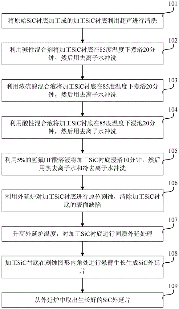
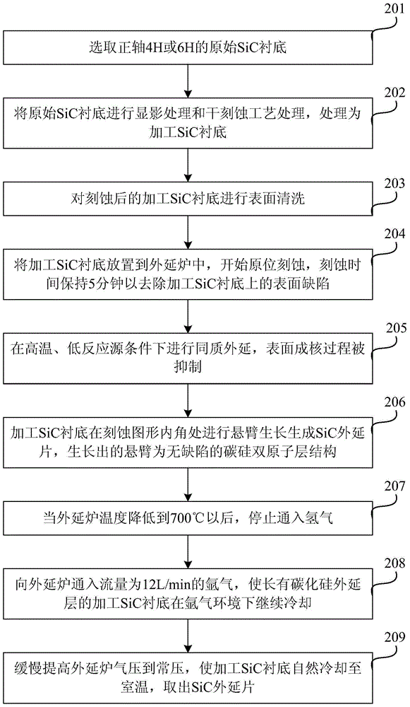
[0027] figure 1 It is a flow chart of embodiment 1 of the etching method for improving Web Growth in the present invention, as shown in the figure, this embodiment specifically includes:

[0028] Step 101, cleaning the processed SiC substrate processed by using the original silicon carbide SiC substrate with positive axis 4H or 6H by ultrasonic;

[0029] Step 102, using an alkaline mixture to boil the processed SiC substrate at a temperature of 85 degrees for 20 minutes, and then rinse it with deionized water;

[0030] Step 103, soaking the processed SiC substrate in a bath at 85 degrees for 20 minutes with a concentrated sulfuric acid mixture, and then rinsing with deionized water;

[0031] Step 104, soak the processed SiC substrate at a temperature of 85 degrees for 20 minutes with an acidic mixed solution, and the...


PUM

PropertyMeasurementUnit
angleaaaaaaaaaa

Abstract

The invention relates to an etching method for improving Web Growth. The method includes: cleaning the processed SiC substrate with ultrasonic, alkaline mixture, concentrated sulfuric acid mixture, acidic mixture, and HF acid solution; using epitaxy The furnace performs in-situ etching on the processed SiC substrate; performs homogeneous epitaxy on the processed SiC substrate; performs cantilever growth at the inner corner of the etched pattern on the processed SiC substrate to form SiC epitaxial wafers, and the grown cantilever is defect-free carbon Silicon double atomic layer structure; the grown cantilever heals to form a carbon silicon double atomic layer film covering the etching mesa area. The invention improves the etching method of Web Growth, realizes the epitaxy of a thin layer of completely defect-free cantilever on the topmost etching table of the positive axis silicon carbide substrate, effectively shortens the epitaxy time and increases the film growth area.

Description

technical field [0001] The invention relates to the technical field of semiconductor materials, in particular to an etching method for improving web growth (Web Growth) Background technique [0002] As one of the representatives of wide band gap semiconductor materials, silicon carbide SiC has superior properties such as large band gap, high breakdown electric field, high thermal conductivity, high electron saturation drift velocity, strong radiation resistance and good chemical stability. It has become a key semiconductor material for the manufacture of a new generation of microelectronic devices and circuits after germanium, silicon, and gallium arsenide. Compared with Si-based devices under the same conditions, SiC-based devices can withstand much higher voltage and microwave power. For example, the ft of SiC MESFET can reach 12-15GHz. [0003] However, there are various defects in SiC that seriously affect the device performance. SiC substrates often inherit these defe...

Claims


Application Information

Patent Timeline
Patent Type & Authority Patents(China)
IPC IPC(8): H01L21/04H01L21/306
Inventor 贾仁需辛斌宋庆文张艺蒙闫宏丽
Owner XIDIAN UNIV
Why Eureka
Try Eureka