Method for manufacturing high-evenness grid electrode lines

A gate line and uniformity technology, applied in semiconductor/solid-state device manufacturing, electrical components, semiconductor devices, etc., can solve problems such as high cost, complicated process, and low production capacity

Active Publication Date: 2013-12-25
SHANGHAI HUALI MICROELECTRONICS CORP
View PDF9 Cites 5 Cited by
  • Summary
  • Abstract
  • Description
  • Claims
  • Application Information

AI Technical Summary

Problems solved by technology

[0008] However, the process of the above scheme is relatively complicated, the

Method used


Image

  • Method for manufacturing high-evenness grid electrode lines
  • Method for manufacturing high-evenness grid electrode lines
  • Method for manufacturing high-evenness grid electrode lines

Examples


Embodiment Construction

[0045] In order to make the content of the present invention clearer and easier to understand, the content of the present invention will be described in detail below in conjunction with specific embodiments and accompanying drawings.

[0046] Figure 4A to Figure 4G A method for fabricating high-uniformity gate lines according to a preferred embodiment of the present invention is schematically shown.

[0047] Specifically, as Figure 4A to Figure 4G As shown, the method for making high-uniformity gate lines according to a preferred embodiment of the present invention includes:

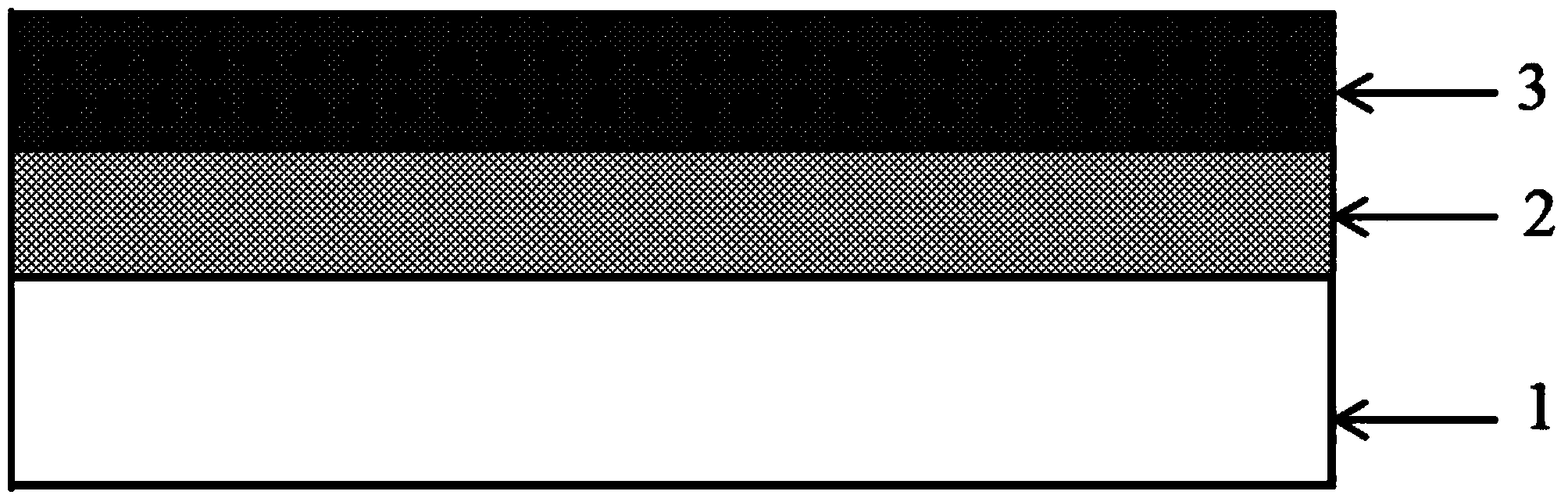
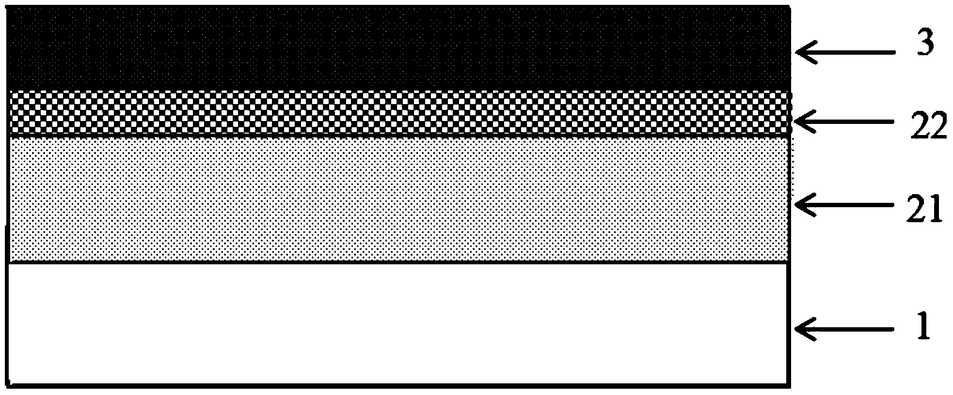
[0048] The first step: on the substrate silicon wafer 1, directly deposit the polysilicon film 4 in sequence, and then directly coat the spin-coated carbon film 21, the silicon-containing hard film 22, and the first photoresist 3 in sequence, such as Figure 4A shown; wherein, it should be noted that the silicon-containing hard film 22 and the first photoresist 3 are combined together as a mask for e...


PUM

PropertyMeasurementUnit
Thicknessaaaaaaaaaa
Thicknessaaaaaaaaaa

Abstract

A method for manufacturing high-evenness grid electrode lines comprises the steps that polycrystalline silicon films are directly deposited on a substrate silicon slice in sequence, then a spin coating carbon film and first photoresist are directly arranged in a coating mode in sequence; exposure and development are carried out, so that the structure of a first grid electrode line is formed in a first photoresist film; the first photoresist is coated with solidification materials with thiocyanic acid salt compounds, cross-linking and solidifying are carried out on the structure of the first grid electrode line in the first photoresist, heating is carried out, so that the solidification materials and the surface of the first photoresist react to form a partitioning film which cannot be dissolved in second photoresist; the first photoresist after solidification is coated with the second photoresist; a first line end cutting pattern is formed in a second photoresist film; the second photoresist film is used as a mask film, the partitioning film and the first grid electrode line are etched, a second line end cutting pattern is formed; the surplus partitioning film and the first grid electrode line are used as a mask film, the spin coating carbon film and the polycrystalline silicon films are etched in sequence continuously, and the structure of a second grid electrode line is formed.

Description

technical field [0001] The invention relates to the field of semiconductor manufacturing, and more specifically, the invention relates to a method for manufacturing high-uniformity gate lines. Background technique [0002] As the integration level of semiconductor chips continues to increase, the feature size of transistors continues to shrink, posing more and more challenges to the photolithography process. The traditional photolithography process usually adopts organic bottom anti-reflective coating (BARC) with polymer materials as the main body to improve the capability of the photolithography process. Figure 1A It is a schematic diagram of the structure of the substrate silicon wafer 1, the organic anti-reflection film 2, and the photoresist 3. The organic anti-reflection film can also expand the adjustable range of the etching process and improve the uniformity of the pattern structure after etching. [0003] After entering the 45nm technology node, it is increasingly...

Claims


Application Information

Patent Timeline
IPC IPC(8): H01L21/28H01L21/027
Inventor 毛智彪
Owner SHANGHAI HUALI MICROELECTRONICS CORP
Why Eureka
Try Eureka